Introduction of Switching Regulators


Ming Sun / October 16, 2022
10 min read • ––– views
Background
Switching Regulators are also called switch-mode power supply (aka SMPS). The main focus in this blog post will be mainly focused on DC-DC switching regulators. Unlike a linear regulator, such as LDO (low dropout), DC-DC converter contains several power FETs which continually switches between full-on and full-off states. The power FETs inside the DC-DC converter does not work in the saturation region.
Nowadays, the battery life becomes more and more important for the mobile applications. Switching regulators are typically used as replacements for linear regulators when higher efficiency, smaller size or lighter weight is required [1].
History[1]
Introduction
So what does a switching regulator look like exactly? Fig. 1 shows the TPS563257 EVB (evaluation board) top view.

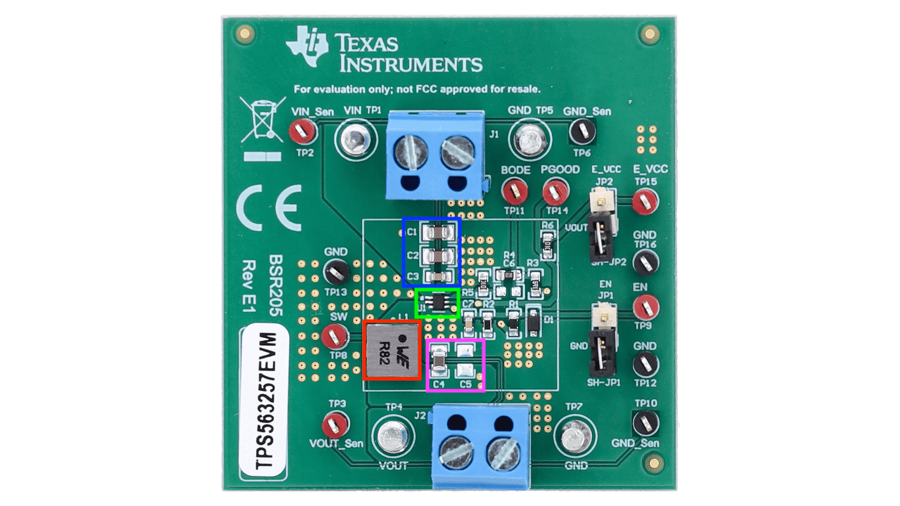
The IC highlighted inside the Green box is TPS563257, synchronous Buck converter in SOT563 package. The input capacitors are highlighted inside the Blue rectangle. The inductor is highlighted inside the Red box, while the output capaictor is highlighted inside the pink rectangle.
The features of TPS563257 are described below:
- 3 V to 16 V input voltage range
- 0.6 V to 7 V output voltage range
- Up to 3 A output Current
- ECO mode and FCCM mode
- Fast transient response
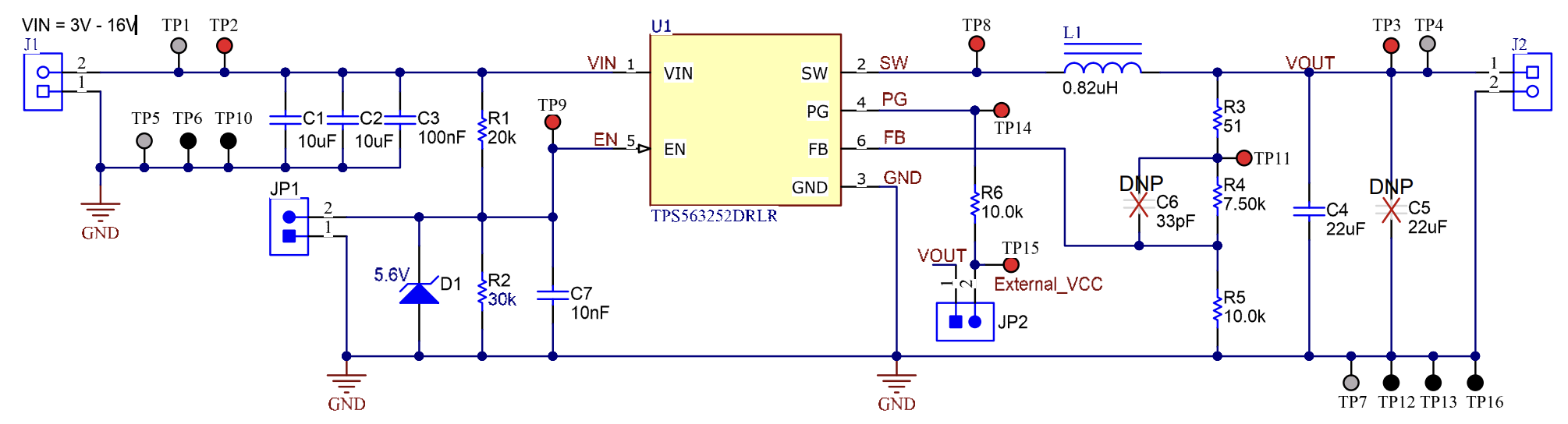
The TPS563252 EVM Schematic is shown in Fig. 2, where VIN is the input power supply, SW is the switching node and VOUT is the output of TPS563252 Buck converter.

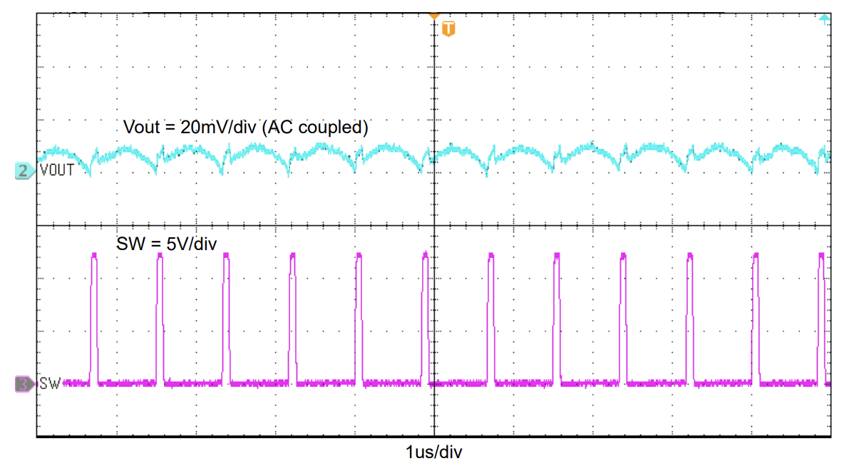
As the name implies, switching regulator uses switching event to maintain regulation of its output voltage. In Fig. 3, the VOUT ripple and SW waveforms are shown.

Control loop
Voltage regulation is achieved by controlling the duty cycle of the DC-DC converters. The most popular control method is peak current mode control in the industry. In general, the control theory can be divided into the linear control method and the ripple-based control method. In the linear control method, the DC-DC converter's power stage is perturbed and linearized. From there, a linear model is derived. Then we can use the control theory, phase margin, gain margin to design the compensator, either Type-II or Type-III compensator for a proper cross-over frequency and phase margin for stability. In the linear control method, we have voltage mode, peak current mode, valley current mode, average current mode and etc.
On the other hand, in the ripple based control method, the DC-DC converters can be considered as a oscillator, whose switching frequency varies based on the input/output condition, loading condition and external components (BoM, bill or material). Some of the popular ripple-based control methods include hysteretic control, constant on time, constant off time, etc.
Topologies
The most popular DC-DC architecture topologies are Buck, Boost and Buck-boost. For Buck, it steps down the input voltage and generates a lower DC voltage at its output. For a Boost converter, it steps up the input voltage and generates a higher DC voltage at its output. For a Buck-boost converter, it can either step up or step down, depending on the input and output voltage level.
References
[1] Switched-mode power supply - Wikipedia
[2] Induction coil - Wikipedia
[4] 1960: METAL OXIDE SEMICONDUCTOR (MOS) TRANSISTOR DEMONSTRATED
[5] The Tektronix 7000 Oscilloscope series
[6] TPS563252 and TPS563257 Step-Down Converter Evaluation Module User's Guide