Popular converters and the conversion ratio derivation


Ming Sun / October 26, 2022
25 min read • ––– views
Among the DC-DC switching regulator topologies, the most popular ones are Buck, Boost and Buck-boost. In this tutorial, we will talk about how each of them works and we will derive their conversion ratio equations by using the voltage-second balance equations for inductors. To keep it simple, we will only focus the conversion ratio derivation for CCM in this tutorial.
For simplicity, assume the switch is ideal, meaning when switch is closed its on impedance is 0Ω, while when switch is open, its impedance is infinity.
The asynchronous topology is used with a free wheeling diode instead of a high-side and low-side power switch.
When free wheeling diode is on, the diode forward voltage VF is zero.
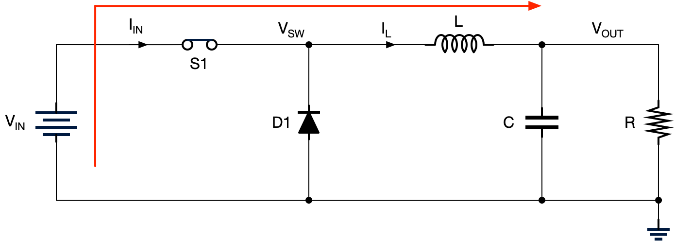
Buck converter
Fig. 1 shows a simple Buck power stage, where a VIN is the input voltage and VOUT is the output voltage of the Buck converter.


Now let us define two time interval as follows. The time interval when switch S1 closed is DTS, while the time interval when switch S1 open is D'TS.
During DTS, S1 is closed. The inductor current IL will flow through S1 to the VOUT.
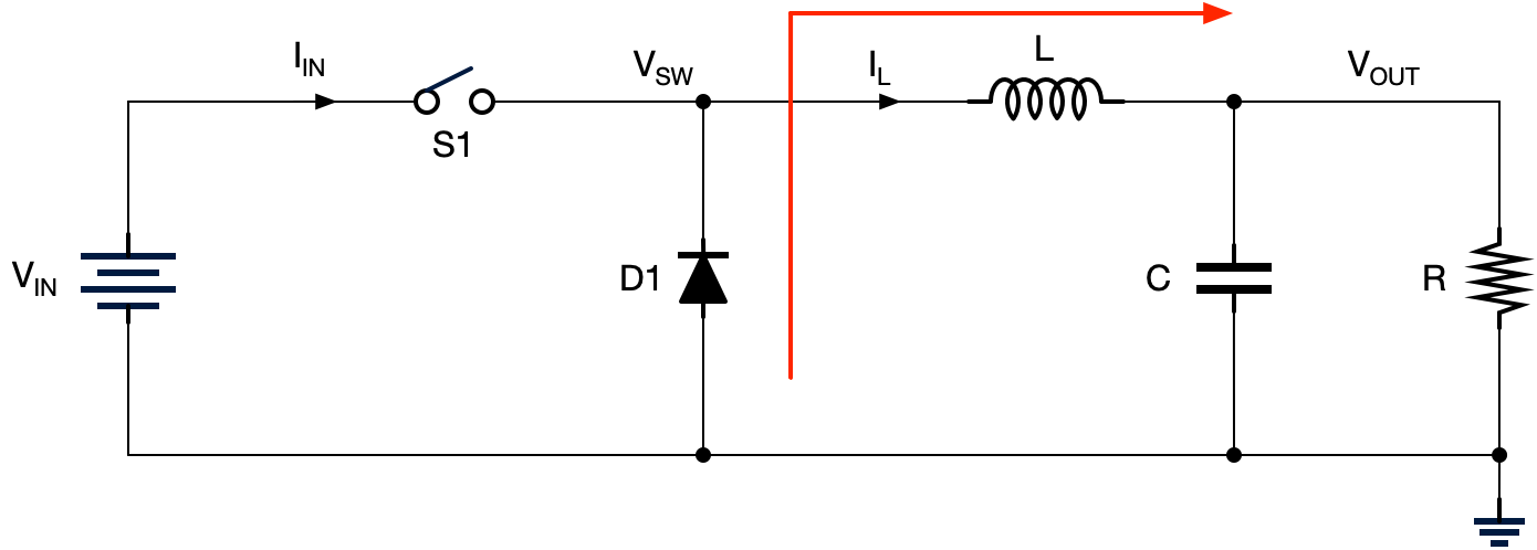
During D'TS, S1 is open. The inductor current IL will flow through diode D1 to the VOUT.
Intuitively, switch S1 will generate a square wave at switching node VSW. The LC filter is just a low pass filter, which will filter out the AC component of the VSW and generate a DC output voltage at VOUT.
The inductor current waveform and the switching node waveform can be sketched as shown in Fig. 4.

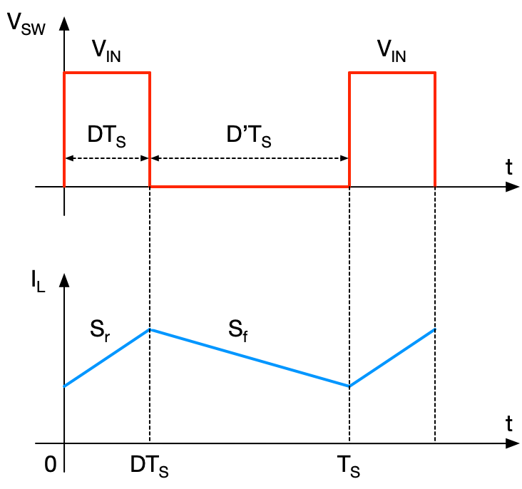
From Fig. 4, we can tell that during the steady state, the inductor current at t=0 should be equal to the inductor current at t=TS, which can be written as:
For inductor, we know that:
Or,
As shown in Fig. 4, during DTS, the voltage across the inductor is constant, which can be calculated as VIN-VOUT. Therefore, the inductor up slope Sr can be calculated as:
Similarly, during D'TS, the voltage across the inductor is constant as well, which can be calculated as -VOUT. Therefore, the inductor up slope Sf can be calculated as:
From Eq. 1, we have:
Where,
Combining Eq. 4~7, we have:
From Eq. 8, the conversion ratio can be calculated as:
Since duty cycle D is between 0 and 1, Buck converter's conversion ratio is always less or equal to 1. As a result, Buck converter can be used to step down the input voltage.
The above process can be summarized as the voltage balance equation for the inductor as follows:
Where, VL,DTS is the voltage across the inductor during DTS. And VL,D'TS is the voltage across the inductor during D'TS.
Boost converter
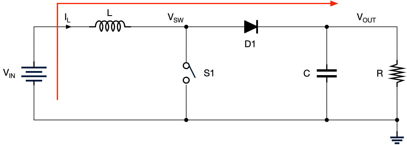
The Boost converter can be used to step up the input voltage to a higher voltage level. Its block diagram is shown in Fig. 5.

Now, we can follow the same procedure to derive the conversion ratio as what we have done for the Buck converter. The DTS is defined as the time interval when the inductor current flows through the switch S1, while D'TS is defined as the time interval when the inductor current flows through free wheeling diode D1.
During DTS, S1 is closed. The inductor current IL will flow through S1 to the ground. During this time interval, the inductor current will ramp up due to the fact that the voltage across the inductor is positive.


During D'TS, S1 is open. The inductor current IL will flow through D1 to the output. Due to the fact that the inductor is not directly connected to the output, Boost converter will have RHPz (right half plane zero) effect, which limits how high the cross over frequency can be. The Boost converter block diagram during D'TS is shown in Fig. 7.
The voltage across the inductor L during DTS can be written as:
The voltage across the inductor L during D'TS can be written as:
Then, we can apply the voltage-second balance equation in Eq. 10. We have:
From Eq. 13, the conversion ratio of the Boost converter can be written as:
Since the termal D' is always between 0 and 1, the Boost converter's conversion ratio is always greater than 1. Therefore, Boost converter can be used to step up the input voltage.
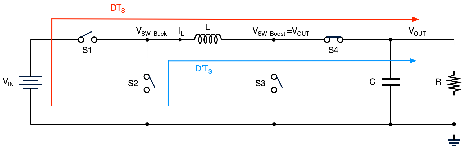
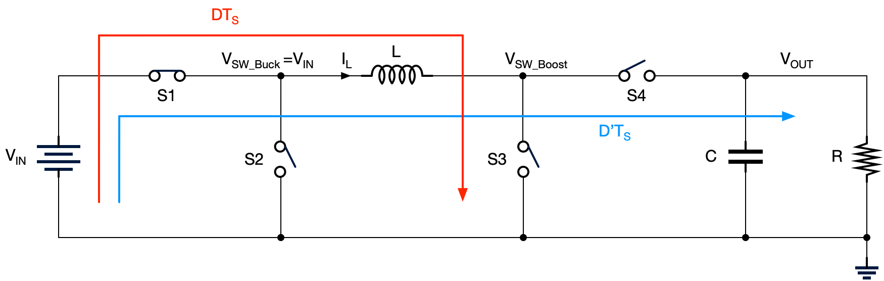
Buck-Boost converter
The Buck-boost converter can be designed with a four switch Buck-or-Boost architecture, which is shown in Fig. 8. Many of the Advanced Low Power Buck-boost converters (such as TPS63xxx) have all four switches integrated in the IC[2].

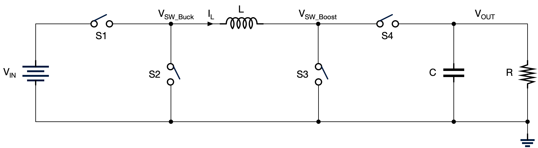
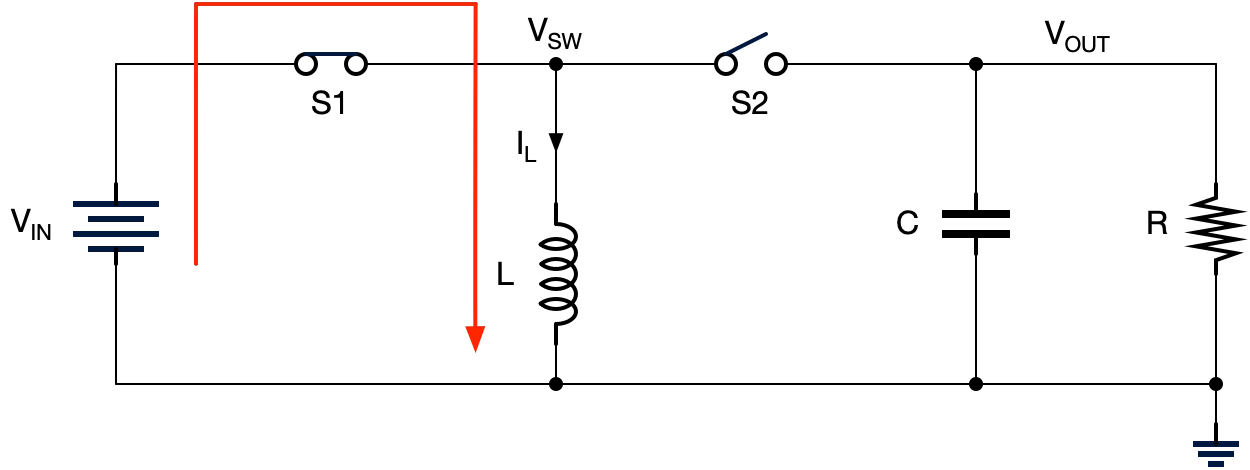
The operation of the four switch Buck-Boost is quite simple. Basically the converter can be configured to work either in Buck mode or Boost mode. For example, if we set switch S4 to be closed all the time, Fig. 8 will become to a Buck converter as shown in Fig. 9.

In Fig. 8, if we set switch S1 to be closed all the time, Fig. 8 will become to a Boost converter as shown in Fig. 10.
The conversion ratio for the Buck mode and Boost mode can be calculated using Eq. 9 and Eq. 14.
Inverted Buck-Boost converter
The Inverted Buck-Boost (IBB) converter can be used to step up or step down the input voltage to a negative voltage. Its block diagram is shown in Fig. 11.


Now, we can follow the same procedure to derive the conversion ratio as what we have done for the Buck converter. The DTS is defined as the time interval when the inductor current flows through the switch S1, while D'TS is defined as the time interval when the inductor current flows through switch S2.
During DTS, S1 is closed. The inductor current IL will flow through S1 to the ground. During this time interval, the inductor current will ramp up due to the fact that the voltage across the inductor is positive.
During D'TS, S1 is open and S2 is closed. The inductor will maintain its current flow direction. As a result, the inductor is going to pull charge out of the output capacitor and generates a negative voltage at IBB output. Similar to Boost converter, eue to the fact that the inductor is not directly connected to the output, IBB converter will also have RHPz (right half plane zero) effect, which limits how high the cross over frequency can be. The IBB converter block diagram during D'TS is shown in Fig. 13.

The voltage across the inductor L during DTS can be written as:
The voltage across the inductor L during D'TS can be written as:
Then, we can apply the voltage-second balance equation in Eq. 10. We have:
From Eq. 17, the conversion ratio of the Boost converter can be written as:
- When duty cycle is at 50%, IBB will generate a negative output whose magnitude is the same as the input.
- When duty cycle is less than 50%, IBB will generate a negative output whose magnitude is less as the input. For example,
- When duty cycle is greater than 50%, IBB will generate a negative output whose magnitude is greater as the input.