Average Switch Model of Buck Power Stage


Ming Sun / October 25, 2022
15 min read • ––– views
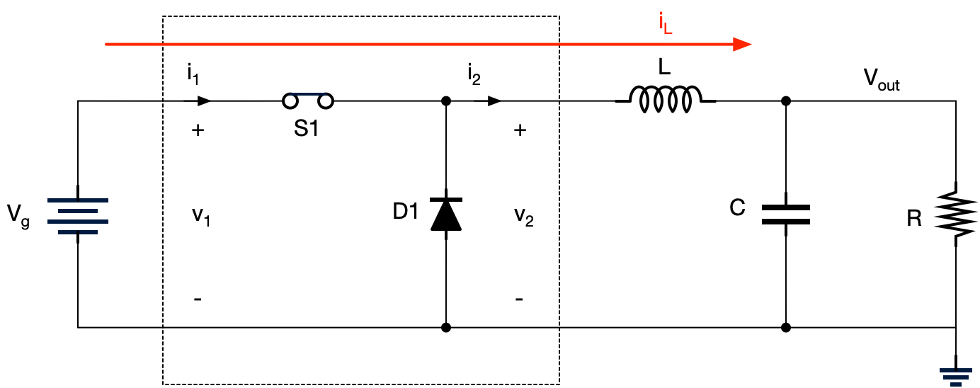
Buck power stage


Fig. 1 shows a non-synchronous Buck power stage, where it contains a switch S1 and a free wheeling diode D1. The target is to derive the averaged switch model as highlighted by the dashed rectangle. The port voltage (v1 and v2) and current (i1 and i2) is defined as shown in Fig. 1 as well.
DC averaged switch model derivation
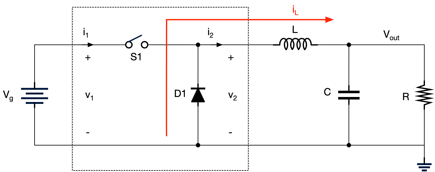
First let us sketch the waveform before calculating the port average voltage and current. To do so, let us re-draw Fig. 1 during DTS and D'TS time interval, where DTS is defined as the time frame when S1 is on and D'TS is defined as the time frame when S1 is off.
During DTS, switch S1 is closed. Inductor current iL flows through switch S1. Because switch S1 is closed, v2 is equal to Vg. As a result, diode D1 is reverse biased and there is no current flowing through it.
During D'TS, switch S1 is open. To maintain a continuous current flow, the inductor will turn on the free wheeling diode D1. If we ignore the forward voltage of D1, v2 will be 0V during D'TS.
Through the analysis of Fig. 2 and Fig. 3, the port voltage and current can be sketched as shown in Fig. 4.


From Fig. 4, we can correlate the average voltage and current information between input port and output port as follows:
From Eq. 1, the DC average switch model can be sketched as shown in Fig. 5.


The DC averaged switch model can be used to derive the conversion ratio in CCM. For example, we can plug in the DC averaged switch model Fig. 5 into Fig. 1. In DC conditions, the inductors are short and the capacitors are open. So Fig. 1 can be re-drawn as shown in Fig. 6.


It is quite obvious that the conversition ratio can be calculated as:
AC averaged switch model derivation
Next, let us derive the AC averaged switch model. To do so, we need to add small signal terms into Eq. 1.
The second order terms are ignored in Eq. (3). For example, d*v1 and d*i2 are ignored and considered to be 0. Using Eq. 3, the AC averaged switch model can be sketched in Fig. 7.


In Fig. 7, we can set the DC terms to be zero to get the AC averaged switch model as shown in Fig. 8.

Buck power stage small model derivation - Gvd
Plugging Fig. 8 into Fig. 1, the Buck power stage AC small signal model can be easily re-drawn as shown in Fig. 9.


Here we are interested of the transfer function Gvd, which is defined from d to vo. As a result, the small signal term vg can be set to 0, as shown in Fig. 10.


From Fig. 10, we have:
Gvd is defined as:
By combining Eq. 4 and Eq. 5, we have:
Eq. 6 can be re-written as:
Where,
Eq. 7 and Eq. 8 matches with the equation shown in Ref. [3], slide 84.
Buck power stage small model derivation - Gvg
To calculate transfer function of Gvg, the small signal term d can be set to 0 in Fig. 9.


From Fig. 11, we have:
Gvg is defined as:
By combining Eq. 9 and Eq. 10, we have:
By combing Eq. 8 and Eq. 11, we have:
Eq. 12 matches with the equation shown in Ref. [3], slide 84.
Gvd and Gvg transfer function summary
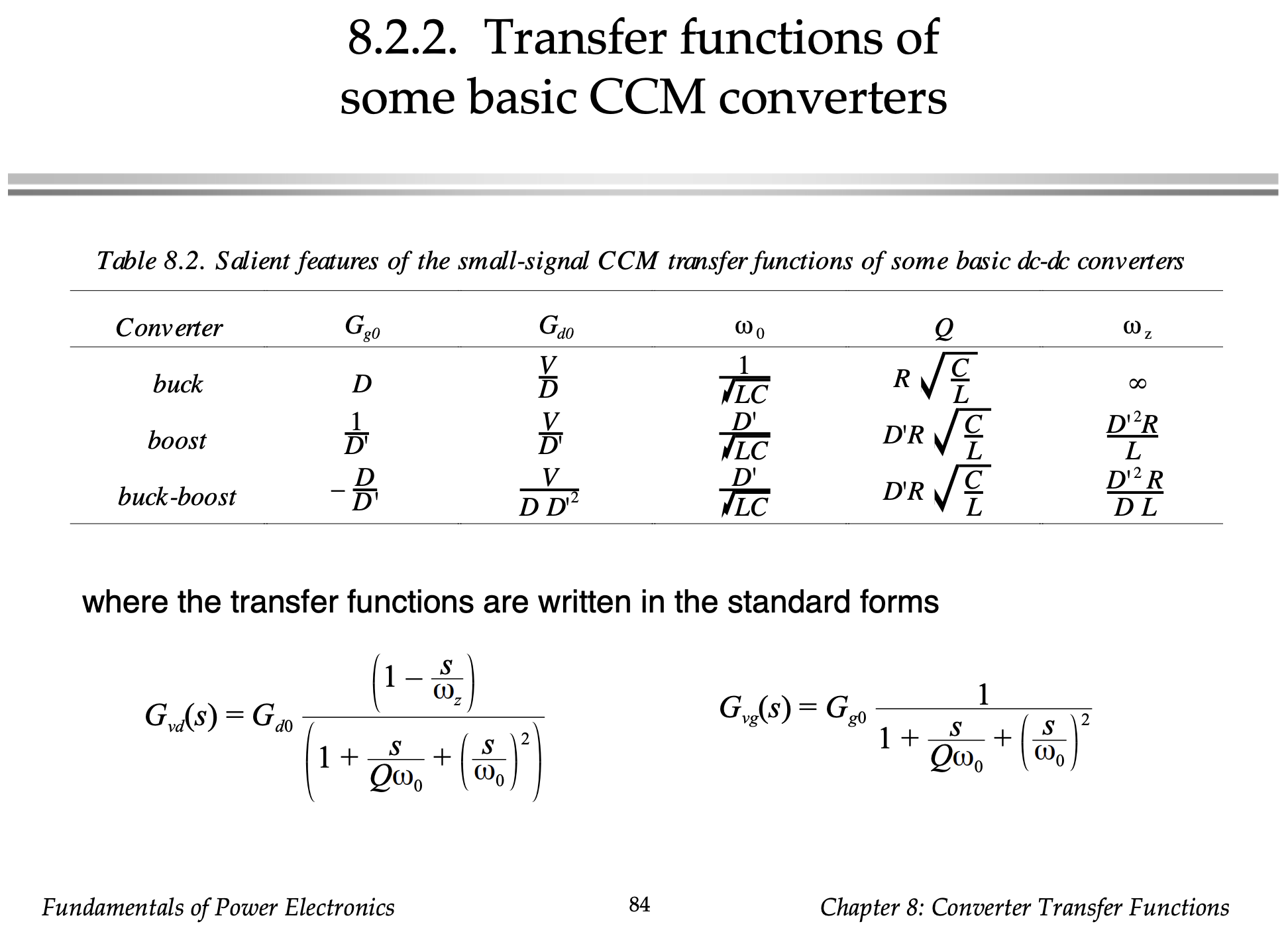
In Ref. [3], the small signal transfer function of Gvd and Gvg for Buck, Boost and Buck-boost are summarized as shown in Fig. 12.

Summary
In this blog post, the derivation of averaged switch model is shown for Buck power stage. A similar derivation process can be applied for Boost and Buck-boost converter as well. The averaged switch model can be used to derive the conversition ratio or the small signal transfer function, which can be super helpful for the control loop design.