Gvd derivation of inverted Buck-Boost (IBB) converter


Ming Sun / November 29, 2022
15 min read • ––– views
Step 1 - construct small-signal equations


Voltage-second balance equation
Fig. 1 shows a synchronous inverted Buck-Boost (IBB) power stage, where it contains a low side switch S1 and a high side switch S2.
For the inductor, we can write the voltage-second balance as[1]:
Where, I is the inductor current, Vg is the Boost converter's input voltage, and V is Boost converter's output voltage Vout. Next, let us perturb and linearize Eq. 1 by introducting the small signal perturbation as:
Here we are trying to derive the transfer function of Gvd. As a result, we can assume Vg is constant. Removing the DC terms from and second order small signal terms Eq. 2 , we have:
Eq. 3 can be written in s domain as:
charge balance equation
For the capacitor, we can write the charge balance as[1]:
Next, let us perturb and linearize Eq. 5 by introducting the small signal perturbation as:
Removing the DC terms and second order small signal terms from Eq. 6, we have:
Eq. 7 can be written in s domain as:
Step 2 - solve the Gvd in Matlab
The Matlab script used to derive the Gvd transfer function is as shown below:
clc; clear; close all;
syms s
syms v i d
syms R L C V Dp I Vg D
syms Gvd Gid
eqn1 = s*L*i == d*Vg + Dp*v - d*V;
eqn2 = s*C*v == -Dp*i + d*I - v/R;
eqn3 = I*Dp == -V/R;
eqn4 = D*Vg + Dp*V == 0;
eqn5 = Gvd == v/d;
eqn6 = Gid == i/d;
results = solve(eqn1, eqn2, eqn3, eqn4, eqn5, eqn6, [v i I Vg Gvd Gid]);
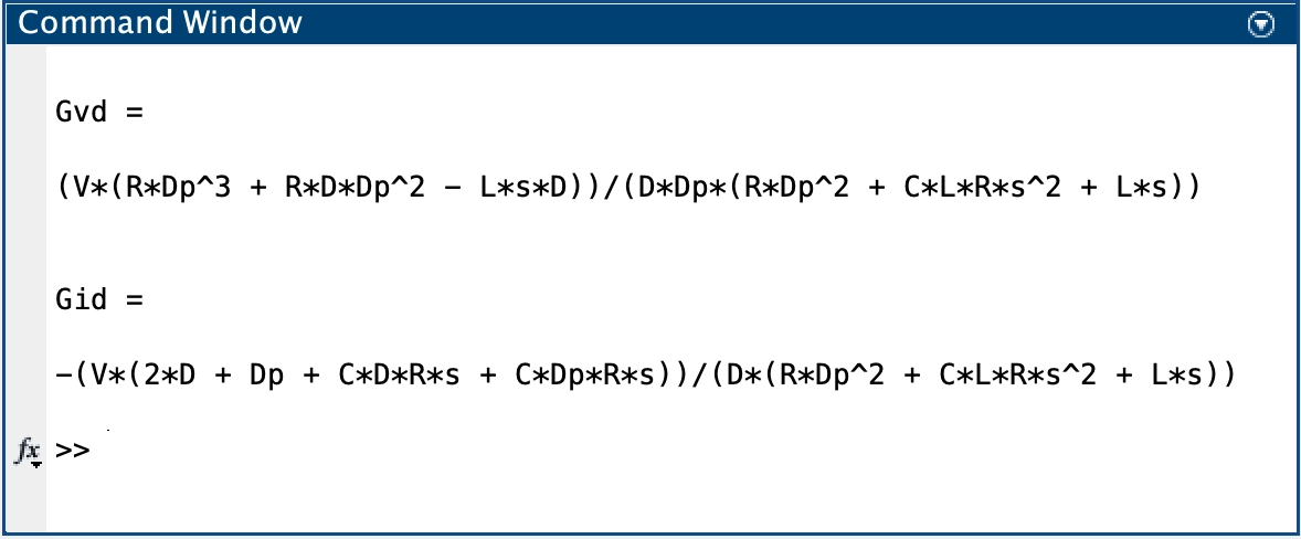
Gvd = simplify(results.Gvd)
Gid = simplify(results.Gid)
Fig. 2 shows the Gvd derived result from Matlab.

Next, we can use wxMaxima to simplify the results as shown in Fig. 3.

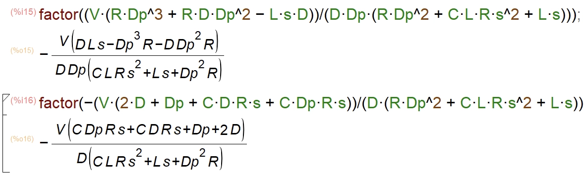
From Fig. 3, we have:
Eq. 9 can be rewritten as:
Simplis for verification of Gvd transfer function
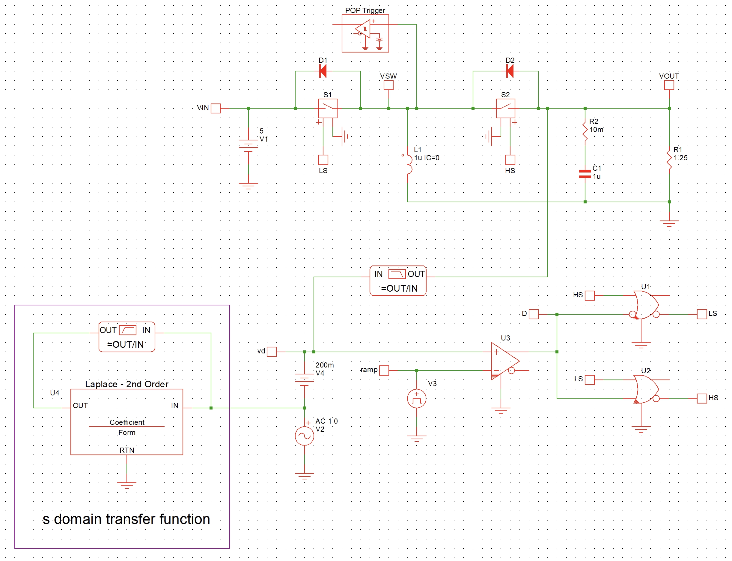
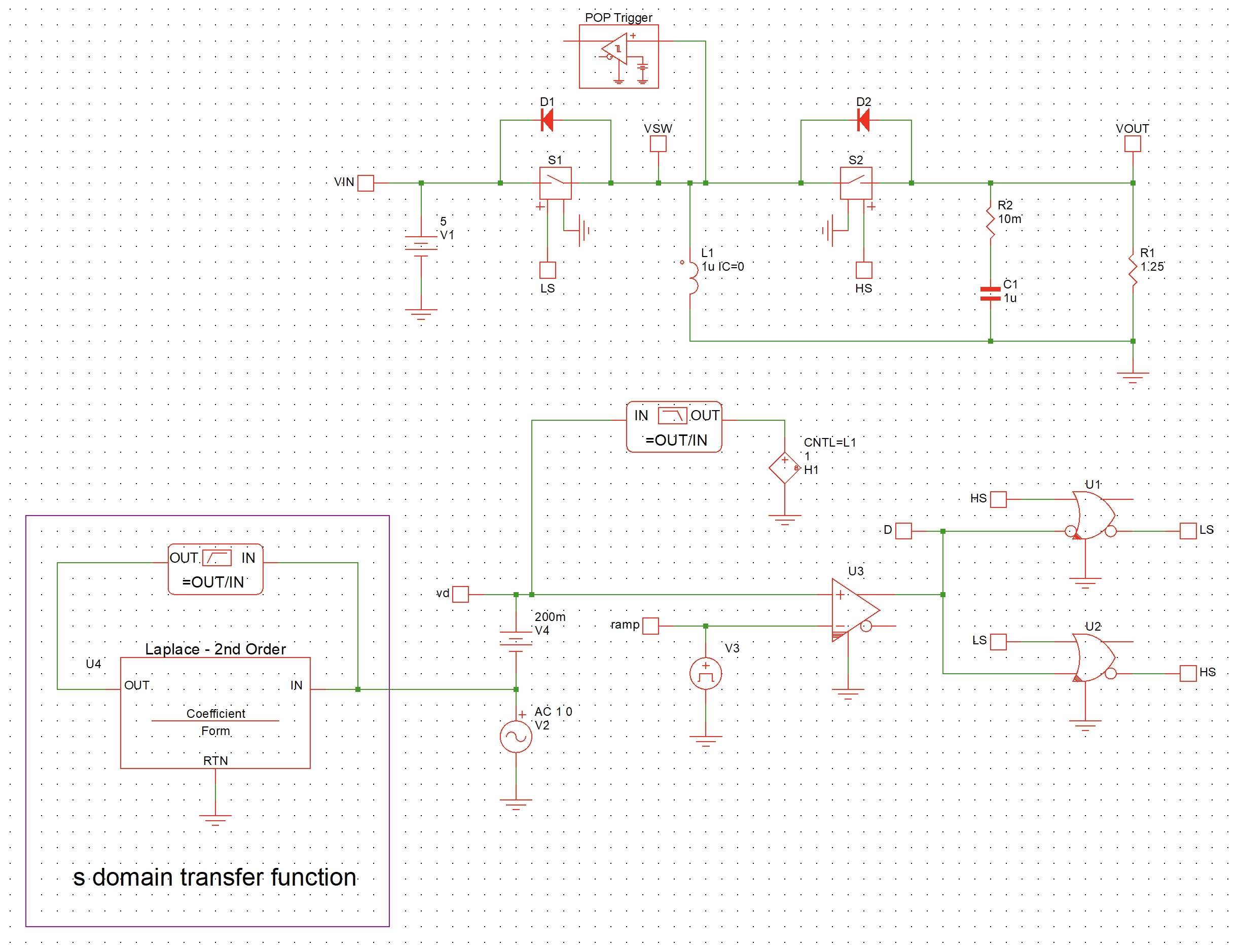
To simulate Gvd transfer function in Simplis, the open loop Boost converter model is as shown in Fig. 4.

To set the property of the Laplace Transfer Function block, Eq. 10 can be re-written as:
We can plug in the inductor, capacitor, resistor, V and D' values into Eq. 11. We have:
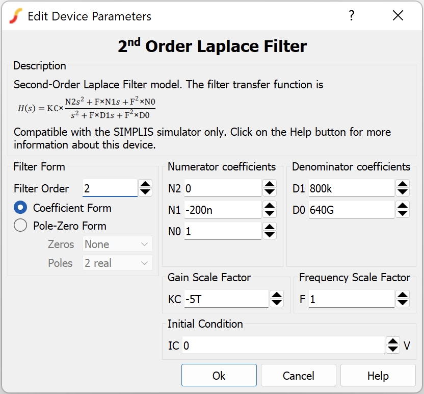
Based on Eq. 11, the property of the 2nd-order Laplace Transfer Function is as shown in Fig. 5.

The Simplis simulation results are as shown in Fig. 6. From Fig. 6, we can see that the mathematical Laplace transfer function matches with the AC simulation results of Gvd very well at low frequency range.

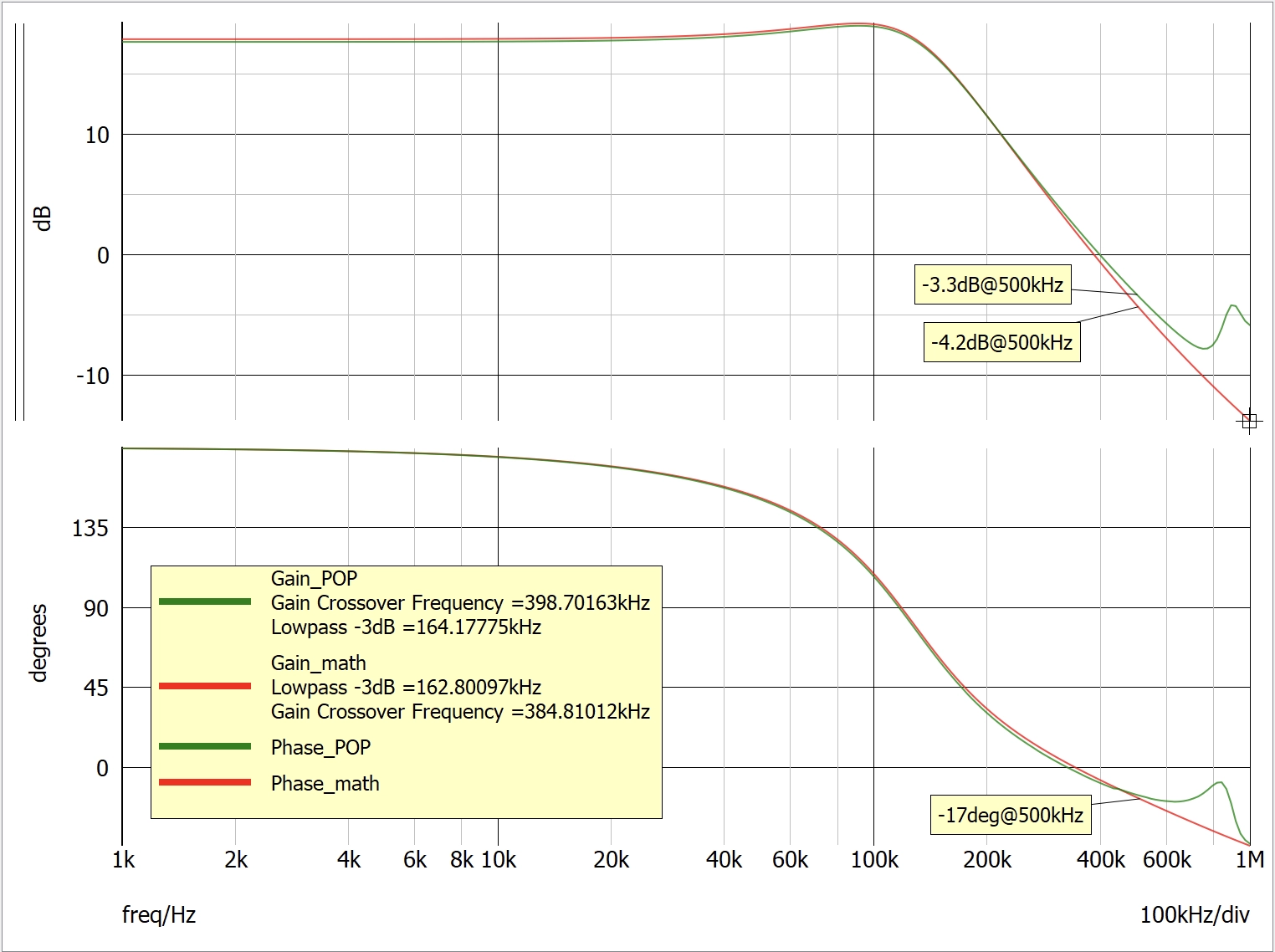
But the difference is small enough and the it will not impact the actual design when we use the mathematical equations since in most of the design the closed loop cross over frequency is much less than the switching frequency fsw.
Gid verification
From Fig. 2, the Gid transfer function can be written as:
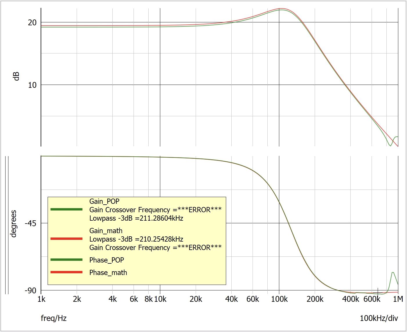
To verify the Gid transfer function, the Simplis test bench can be modified as shown in Fig. 7.

To set the property of the Laplace Transfer Function block, Eq. 12 can be re-written as:
We can plug in the inductor, capacitor, resistor and Vg values into Eq. 13. We have:
Based on Eq. 14, the property of the 2nd-order Laplace Transfer Function is as shown in Fig. 8.


The Simplis simulation results are as shown in Fig. 9. From Fig. 9, we can see that the mathematical Laplace transfer function matches with the AC simulation results of Gid.

References and downloads
[1] Fundamentals of power electronics - Chapter 2
[2] Open-loop IBB converter model for Gvd simulation in Simplis - pdf
[3] Open-loop IBB converter model for Gvd simulation in Simplis - download
[4] Open-loop IBB converter model for Gid simulation in Simplis - pdf
[5] Open-loop IBB converter model for Gid simulation in Simplis - download