Open loop Buck converter in Simplis


Ming Sun / November 28, 2022
17 min read • ––– views
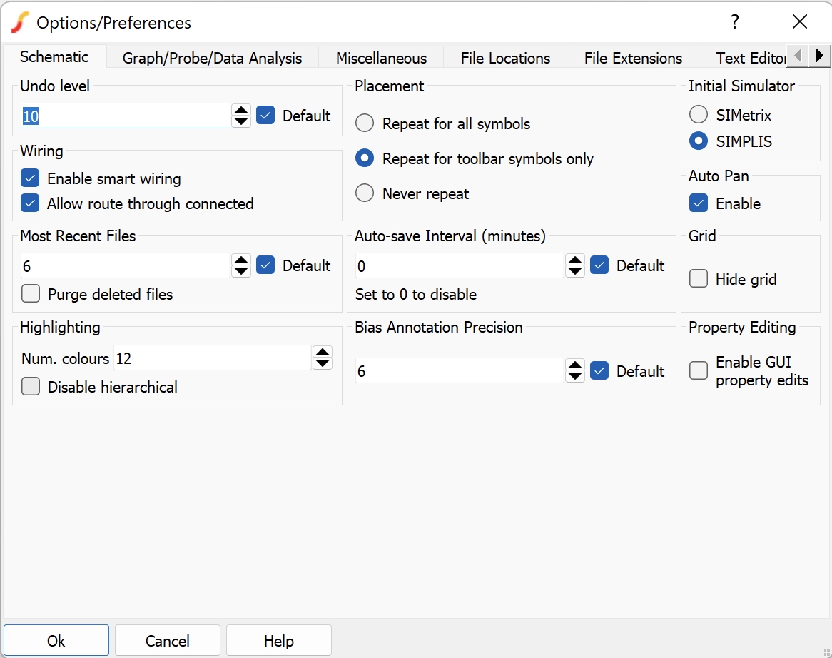
Setting up Simplis as the default simulator[1]
Go to File => Options => General.... Then choose SIMPLIS as the Initial Simulator. Then click OK to apply the change.

Import the corresponding components
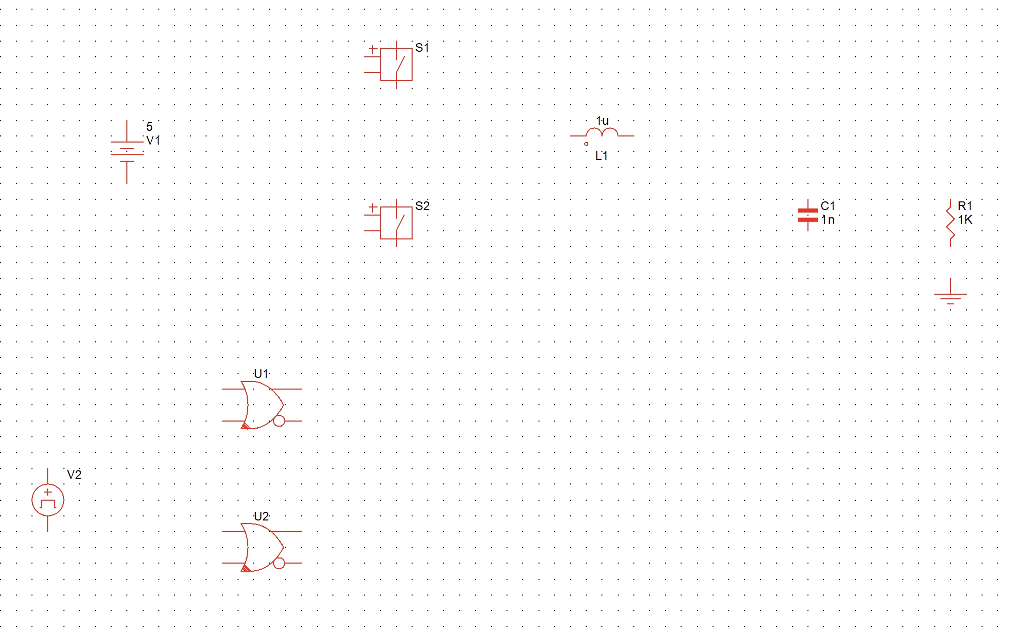
First, let us try to import the following components to the schematic.

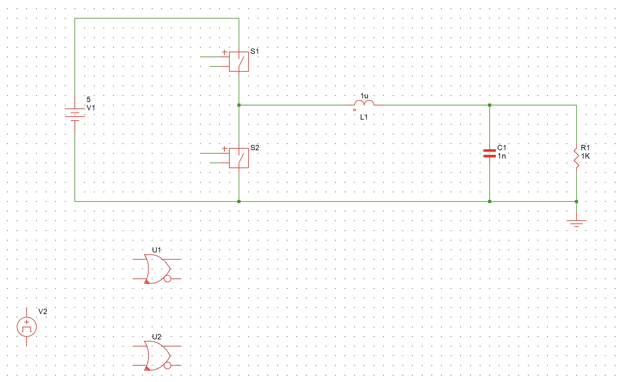
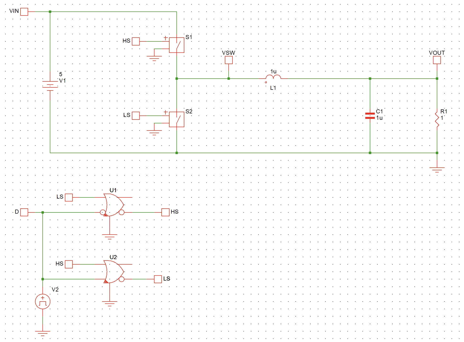
Connect and wiring
Next, let us connect the components as shown in Fig. 2.
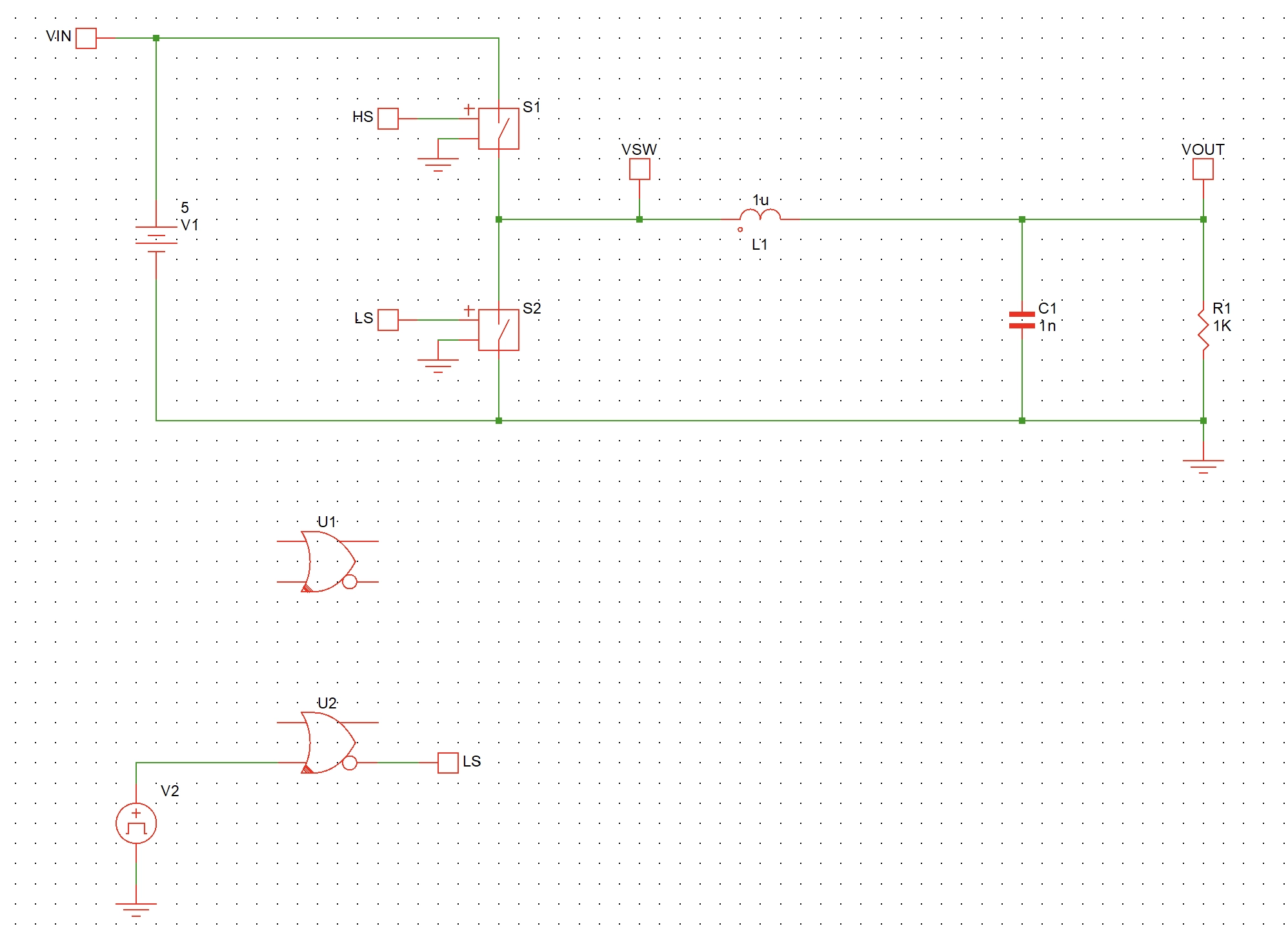
Add Terminal
To reduce the number of wires on the schematic, we can use Terminal to connect the same nets as shown in Fig. 3.

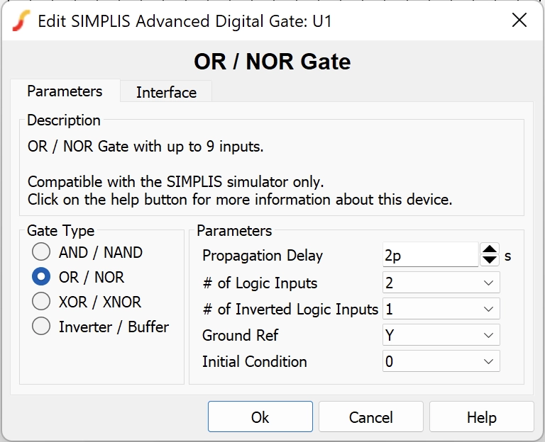
Reconfig NOR2 gate
Double click U1 (NOR2 gate) and change one of its input to be the inverted logic input as shown in Fig. 4.


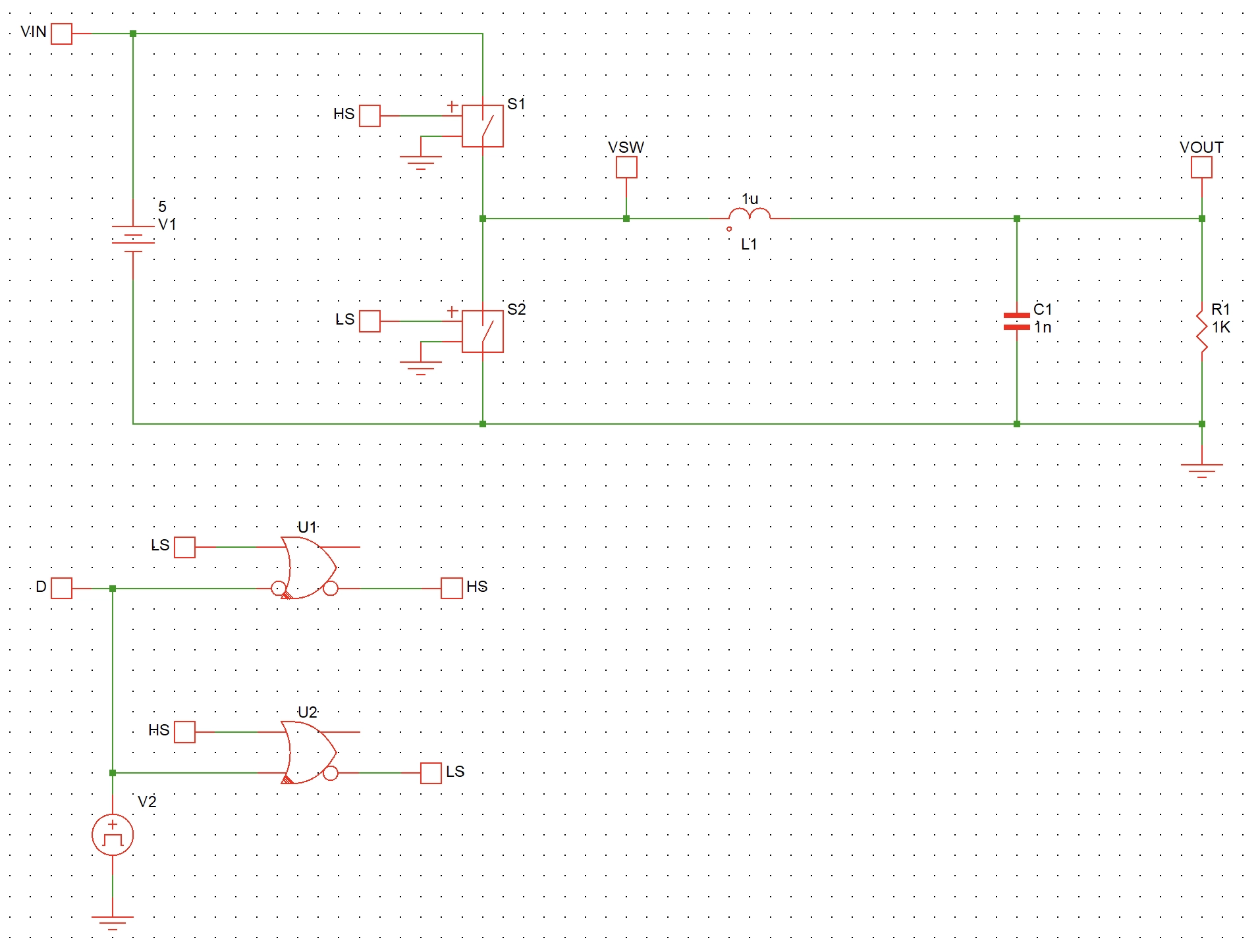
Connect the driver with BBM architecture
Basically, we are trying to create a simple driver with BBM function. BBM means Break-before-make, which is a widely used technique in power stage driver design to prevent the shoot-through current between the high-side and low-side power FETs.
The schematic is as shown in Fig. 5. When D is equal to logic 1, LS will be set to logic 0, regardless the state of HS. As a result, the low side power FETs S2 is first turned off. When both LS and D are at logic 0, HS will be set to logic 1 and high side power FETs S1 will be turned on.

Change component properties
Let us change the component properties as shown in Fig. 6.
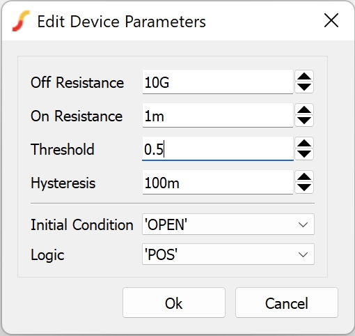
For power FETs S1 and S2, let us change the properties as shown in Fig. 7. Basically, when S1 and S2 are on, the Rdson is set to be 1mΩ. When S1 and S2 are off, the off state impedance is set to be 10GΩ.

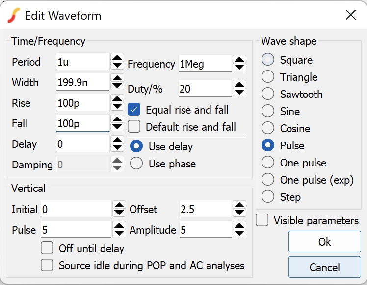
Next, let us modify the waveform generator's properties as shown in Fig. 8. Here, we set it to be a pulse, with 5V amplitude, 1MHz switching frequency and 20% duty cycle.

Choose Transient simulation
Let us run a transient simulation first. Go to Simulator => Choose Analysis...

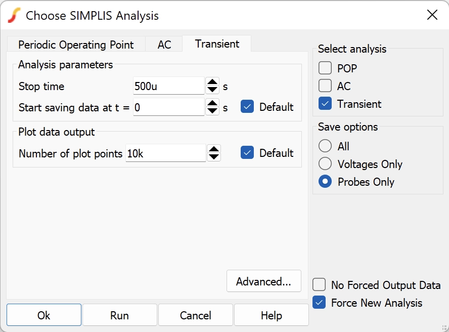
Then click the run button. An error has occured and complains about the ground reference for the NOR2 gate.

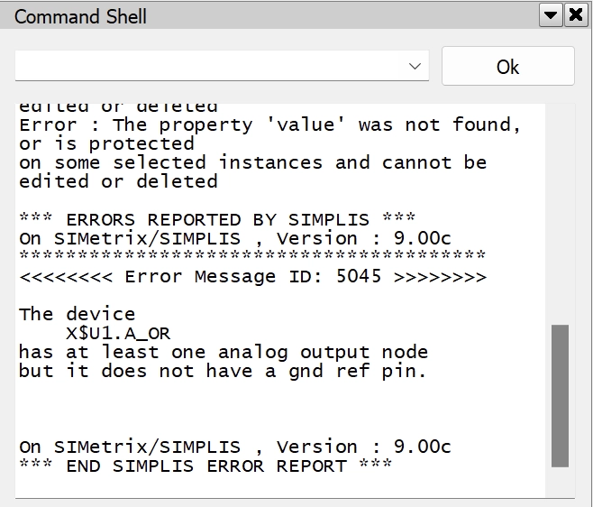
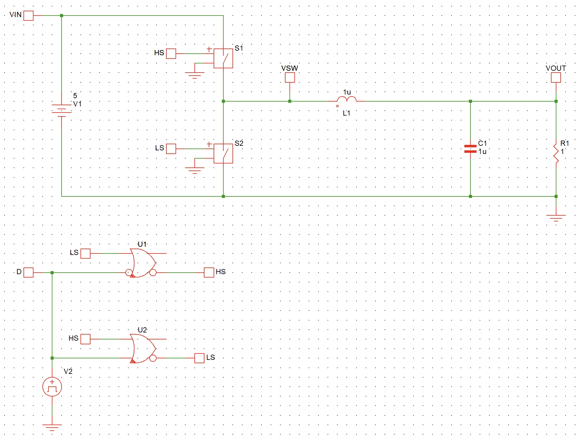
To solve this error, let us double click the NOR2 gate and add one ground reference terminal by setting the Ground Ref property to Y.

Next, let us connect the ground ref terminal to the actual ground. The updated schematic is as shown in Fig. 12.

Click the Run button again and we see that there is no error message pop up.
View transient simulation waveform
At the tool bar, click the Probe Voltage (interactive) button and then click the VOUT net.


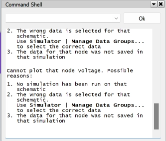
From the command shell, it complains that there is no simulation data available for VOUT net.

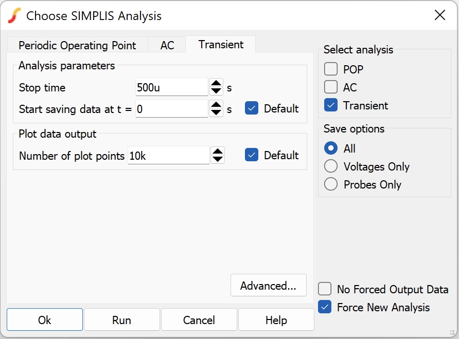
To solve this, in the transient simulation analysis window, let us choose All for the Save options as shown in Fig. 15.

Then click the Run button. The transient simulation results are as shown in Fig. 16.

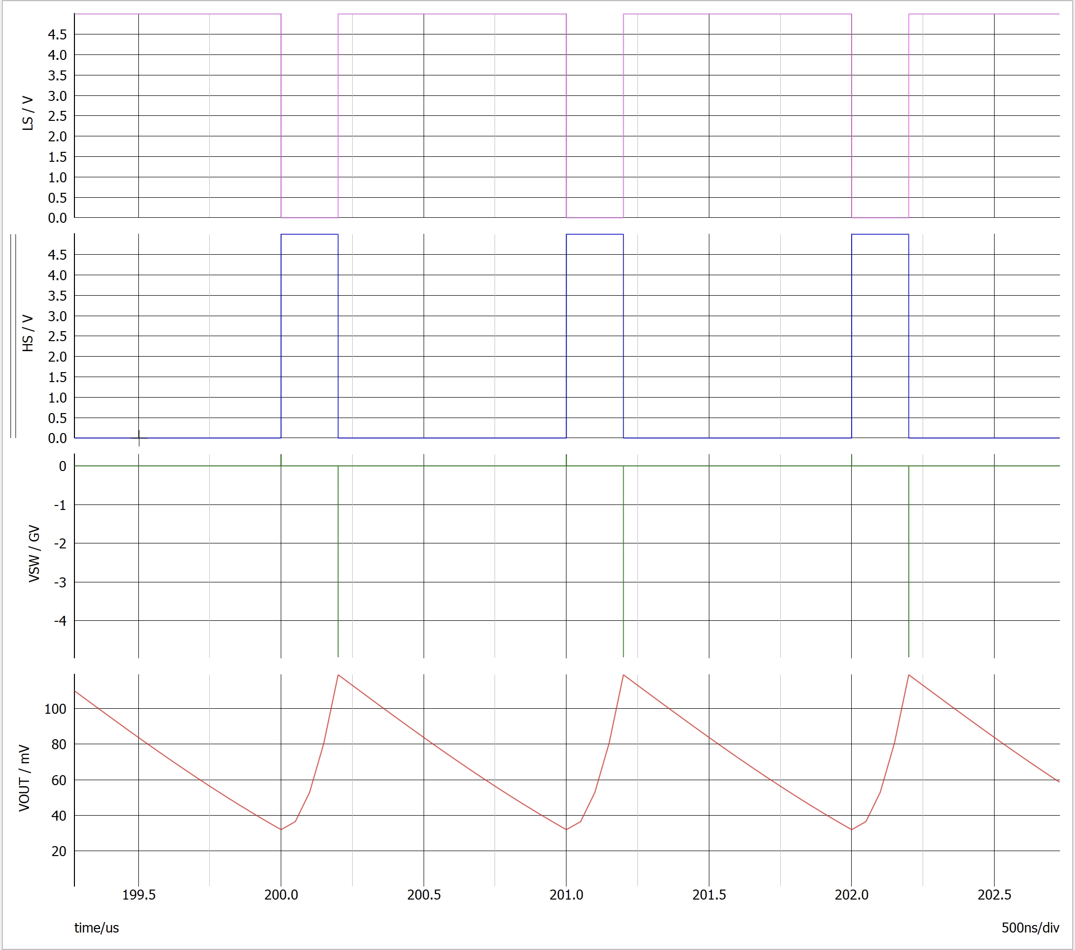
Notice that VSW goes to GV during the dead time. This is because that for the ideal switch S1 and S2, during the dead time since both of them are off, there is no path available for the inductor to flow. To solve this issue, let us add two diodes in parallel with power FETs S1 and S2 switches as shown in Fig. 17.

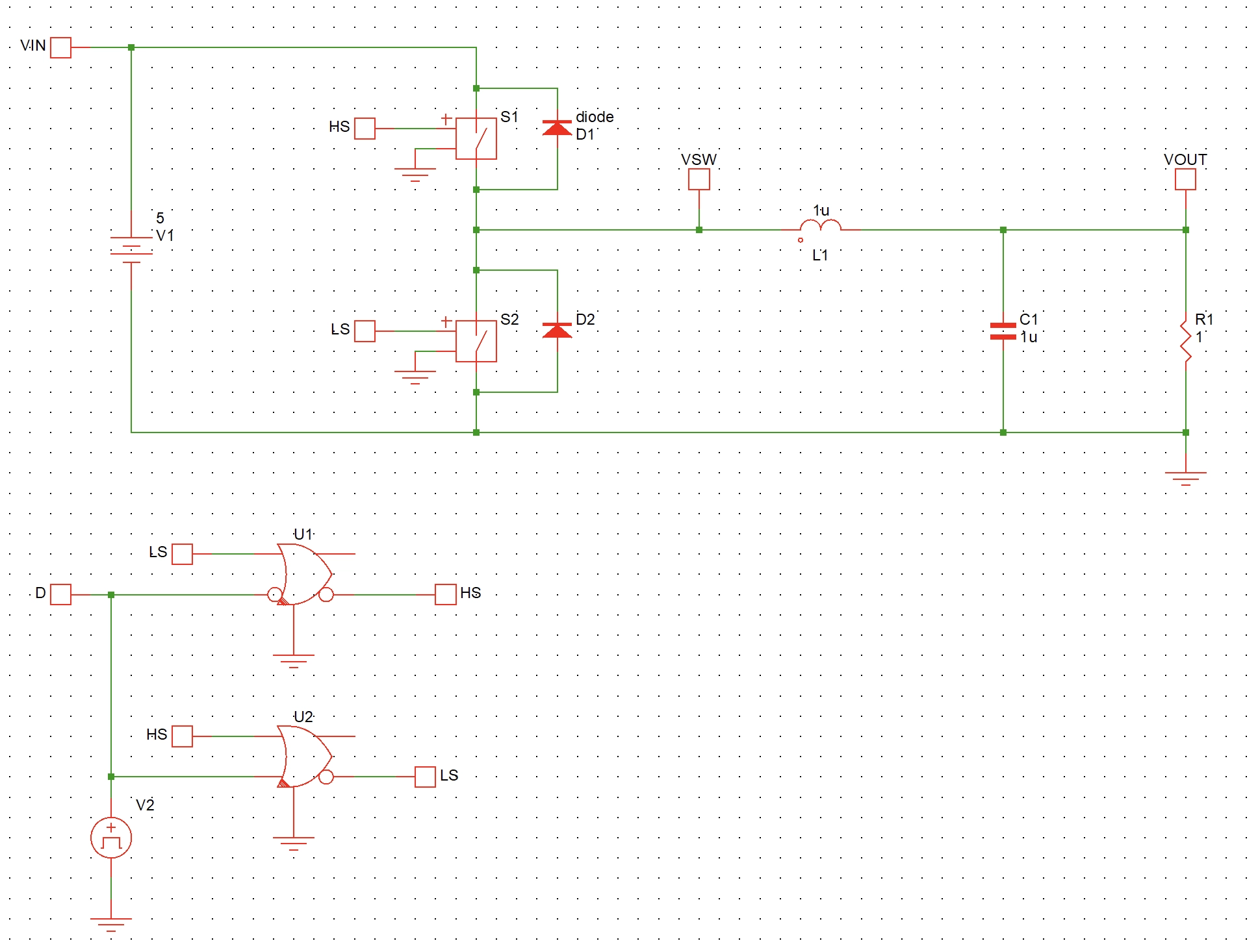
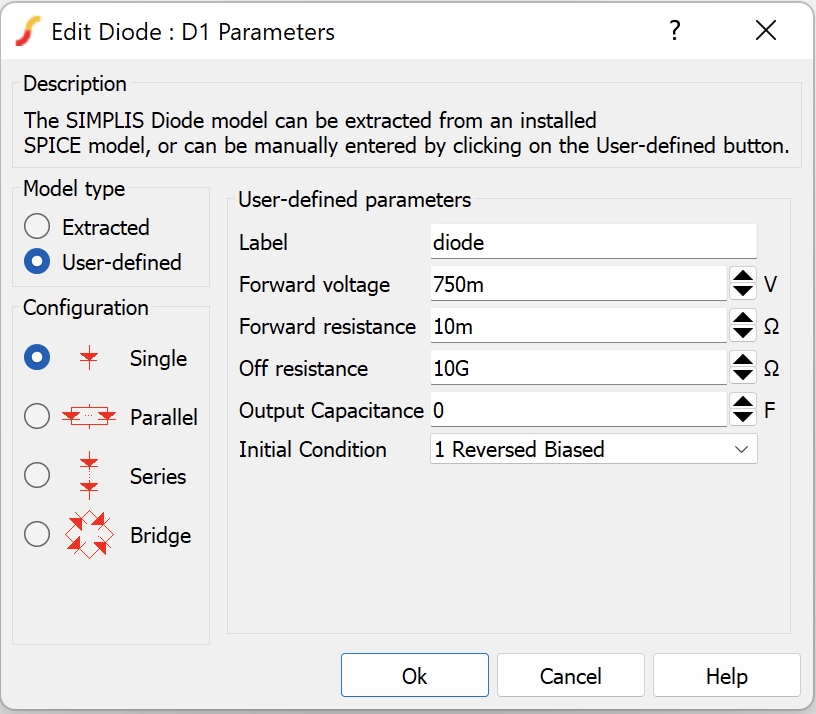
The properties of the diode D1 and D2 are as shown in Fig. 18.

Run the simulation again and the simulation results are as shown in Fig. 19.

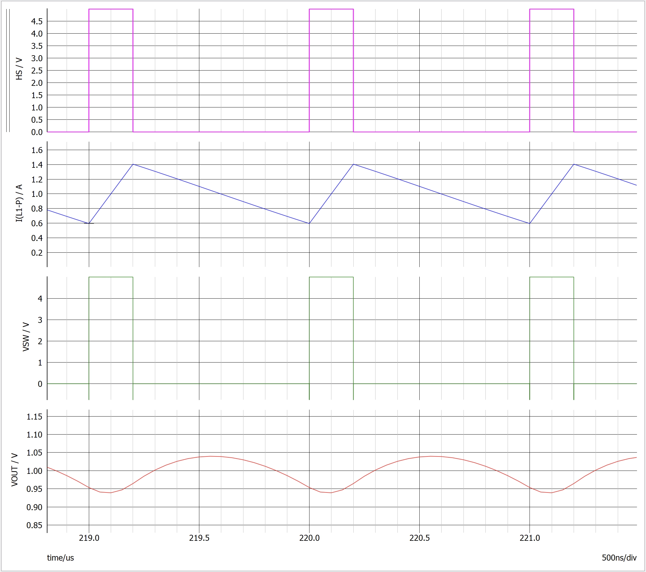
For a Buck converter with 5Vin and 20% duty cycle, its output voltage in CCM can be calculated as 5V*20%=1V, which matches with the simulated results as shown in Fig. 19.
References and materials
[1] SIMPLIS Tutorial