OTA based Type-II compensator transfer function derivation


Ming Sun / December 08, 2022
12 min read • ––– views
Type-II compensator - OTA based
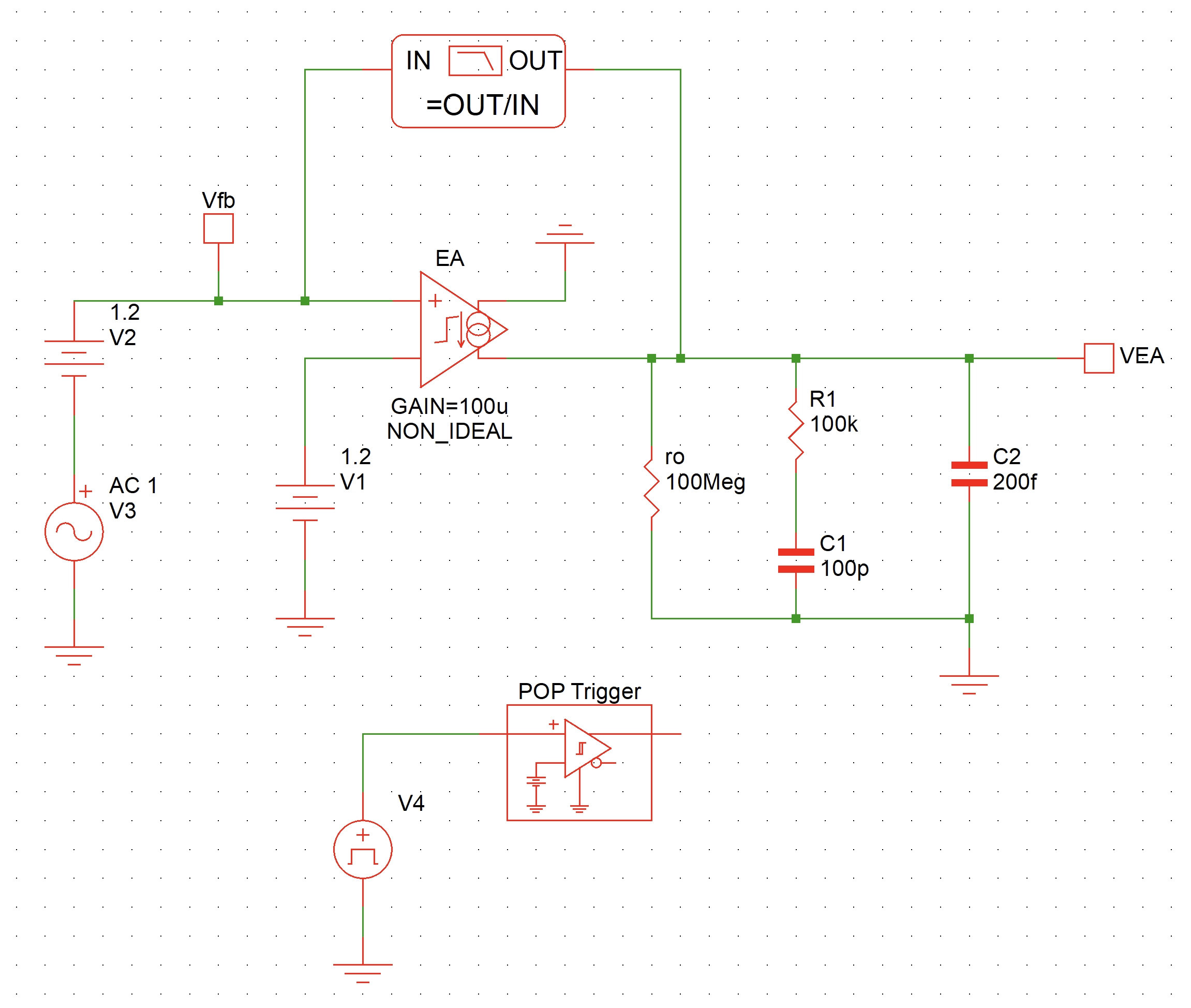
Fig. 1 shows a Type-II compensator, where an OTA is being used.


The transfer function of Type-II compensator is defined as:
The small signal AC model is as shown in Fig. 2, where Vref is set to be AC ground.


The Matlab script used to derive the transfer function of Eq. 1 is as shown below.
clc; clear; close all;

syms Vea Vfb H
syms ro R1 C1 C2 gm s

eqn1 = -gm*Vfb == Vea/ro + Vea*s*C2 + Vea/(R1+1/s/C1);
eqn2 = H == Vea/Vfb;

results = solve(eqn1,eqn2,[Vea,H]);

H = simplify(results.H)

pretty(H)
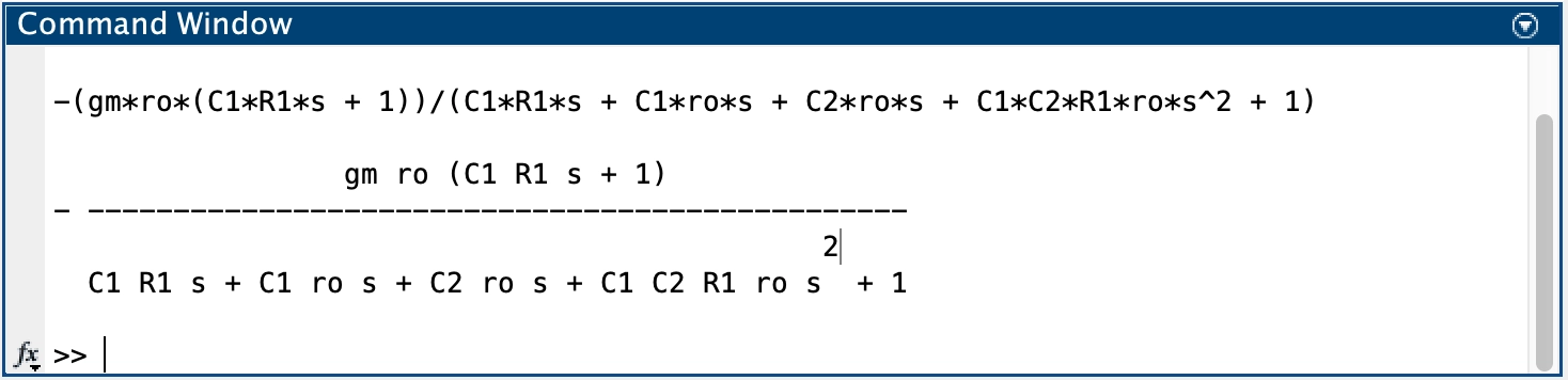
The Matlab derived results are as shown in Fig. 3.

Here, let us assume that capacitor C1 is much larger than capacitor C2 and OTA output impedance ro is much larger than resistor R1. Then, we can use wxMaxima to further simplify the result as shown in Fig. 4.

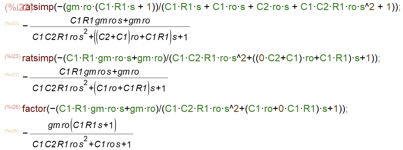
From Fig. 4, we have:
The zero location can be easily calculated to be:
Next, let us derive the pole locations. The denominator can be written as:
Assuming the two poles are far away separated from each other,
Therefore, we have:
By comparing the s and s2 coefficient between Eq. 6 and Eq. 4, we have:
As a result, the pole locations can be calculated as:
As long as OTA output impedance ro is much larger than resistor R1, Eq. 8 result shall be valid.
Simplis verification
The Type-II compensator test bench in Simplis is as shown in Fig. 5.

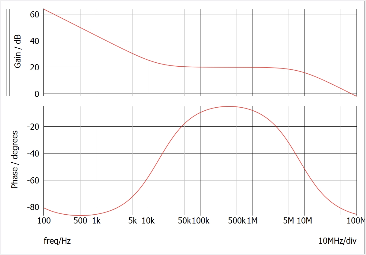
The AC simulation results from Simplis is as shown in Fig. 6.

The following Matlab script is used to compare the Bode plot between Eq. 2 and Simplis simulatio results.
clc; clear; close all;

gm = 100e-6;
ro = 100e6;
R1 = 100e3;
C1 = 100e-12;
C2 = 200e-15;

z = 1/R1/C1;
p1 = 1/ro/C1;
p2 = 1/R1/C2;

s = tf('s');

H = gm*ro*(1+s/z)/(1+s/p1)/(1+s/p2);

h = bodeplot(H);
setoptions(h, 'FreqUnits', 'Hz');   % change frequency scale from rad/sec to Hz
set(findall(gcf,'type','line'),'linewidth',2)
grid on;
hold on;

% read simplis simulation results from csv file
data = csvread("simplis.csv", 1, 0);
freq = data(:,1);
mag = data(:,2);
phase = data(:,3);

ax = findobj(gcf, 'type', 'axes');
phase_ax = ax(1);
mag_ax = ax(2);


% append simplis plot to bode plot
plot(phase_ax, freq, phase, 'r--', 'LineWidth', 2);
plot(mag_ax, freq, mag, 'r--', 'LineWidth', 2);
legend('Math', 'Simplis')
The comparison between Mathematical derivation and Simplis AC simulation results are as shown in Fig. 7.


Summary
Fig. 8 visually check the components which generate poles and zero.

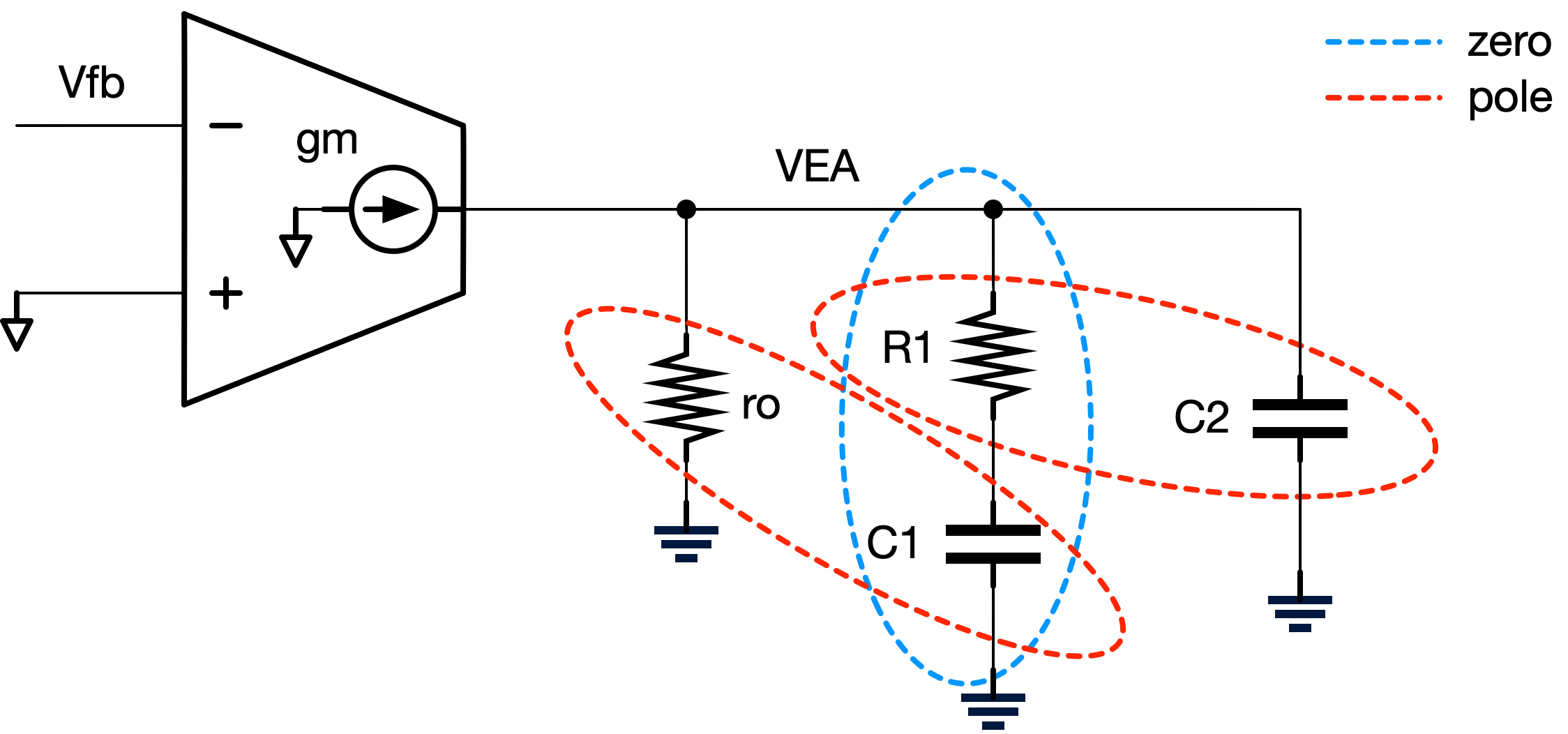
- At low frequency, ro and C1 forms the dominant pole. This pole behaves sort of as the integrator. The high DC gain guarantees the DC regulation accracy of switching regulators.
- At mid-band frequency, R1 and C1 generates a zero, which is going to provide the phase boost in mid-band frequency.
- When frequency becomes higher, capacitor C1 becomes short. Therefore, the mid-band DC gain can be calculated as gmR1. Also, resistor R1 and C2 generates a high frequency pole, which can be used to damping the ripple around switching frequency.
The Bode plot illustration is as shown in Fig. 9.


References and downloads
[1] Demystifying Type II and Type III Compensators Using OpAmp and OTA for DC/DC Converters
[2] Opamp based Type-II compensator test bench in Simplis - pdf
[3] Opamp based Type-II compensator test bench in Simplis - download