Simulation of open-loop switching regulators in Xschem


Ming Sun / November 16, 2022
8 min read • ––– views
Test bench
The simulation test bench is as shown in Fig. 1.

Please refer to Ref. [1] if you would like to view the schematic more clearly in SVG format.
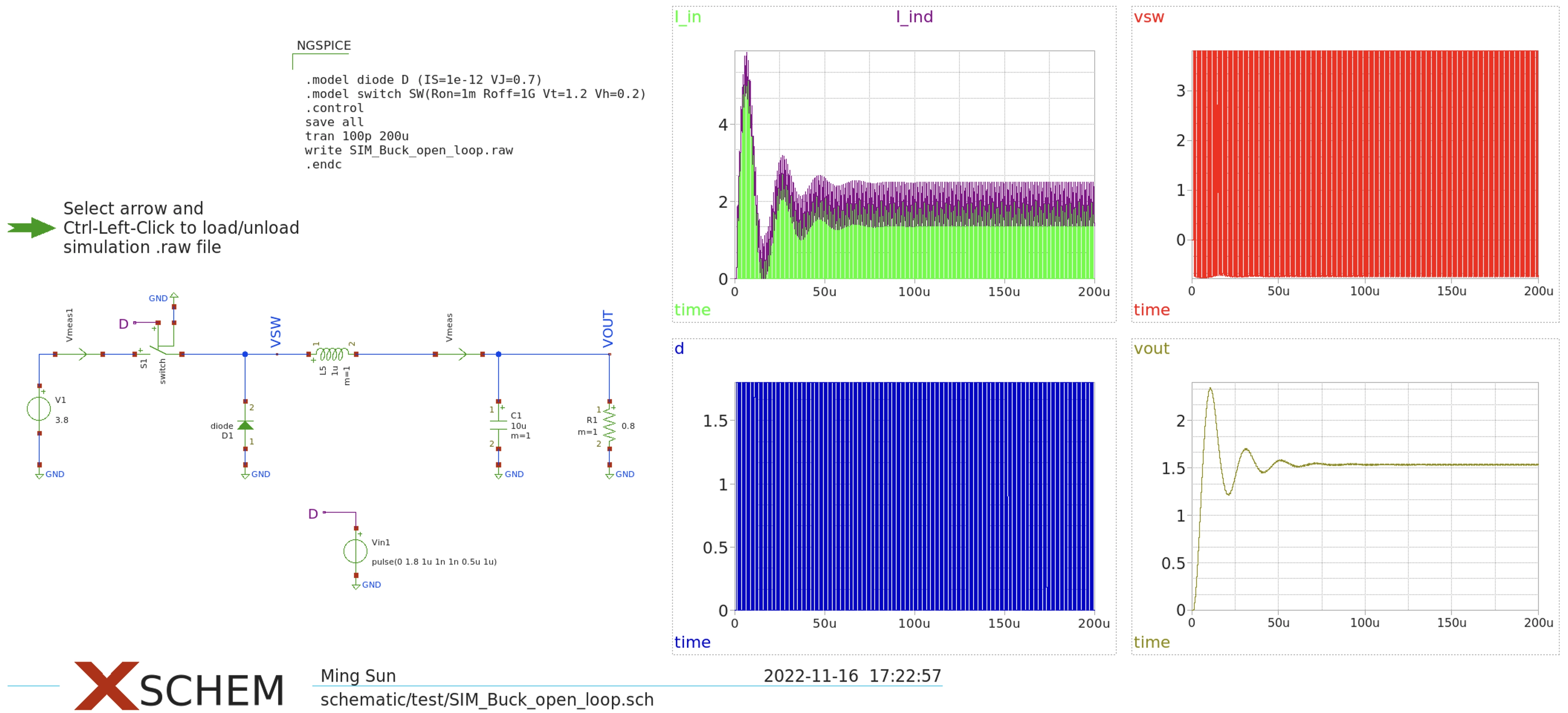
Power stage - asynchronous
Fig. 2 shows the asynchronous Buck power stage. The high side is an ideal switch whose Rdson is 1mΩ when it is on. The switch's symbol and its path is listed below.
symbol: switch_ngspice.sympathorlibrary: xschem_library/devices
name=S1 model=switch
The switch model is named as switch. To define this switch model, we need to put the following script into the code_shown.sym stimulus block.
model switch SW(Ron=1m Roff=1G Vt=1.2 Vh=0.2)


We use a pulse voltage source to control the duty cycle of switch S1. The pulse is defined to be 1MHz clock with 50% duty cycle. For an ideal Buck converter, we know that:
So ideally the Buck converter shall generate a 3.8V*50%=1.9V output. However, from Fig. 1, for simplity, we are using a diode as the low side device for the Buck converter. There will be a conduction loss when the HS is off. So the Vout voltage shall be lower than 1.9V. From the simulation results, we can tell that Vout is about 1.6V.
Simulation results
The zoomed-in waveform is as shown in Fig. 3.


When d=1.8V, the high side switch is on. The differential voltage across the inductor is Vin-Vout. Therefore, inductor current (pink waveform) will start to ramp up. The input current is equal to the inductor current when the high side switch is on. When the high side switch is off, the input current is 0. Due to the pulsating current nature, the input cap for a Buck converter is more critical than the output cap.
Synchronous Buck converter
Fig. 4 shows a synchronous Buck converter macro model. Comparing with Fig. 1, the Buck low side has been changed to an ideal switch.


Fig. 5 shows a zoom-in view of the synchronous Buck power stage.


The diode D1 and D2 are added to make sure during the dead time, there is current path for the inductor current to flow. The zoom in waveform is as shown in Fig. 6.


Comparing with Fig. 3, VSW voltage is 0V when low side is on, instead of -0.7V. As a result, the losses are almost 0, which makes the Vout is 1.9V as predicted by Eq. 1.
References and materials
[1] Asynchronous Buck converter schematic in SVG format
[2] Asynchronous Buck converter schematic download