Voltage-mode Buck converter design example


Ming Sun / December 10, 2022
7 min read • ––– views
LM21215A
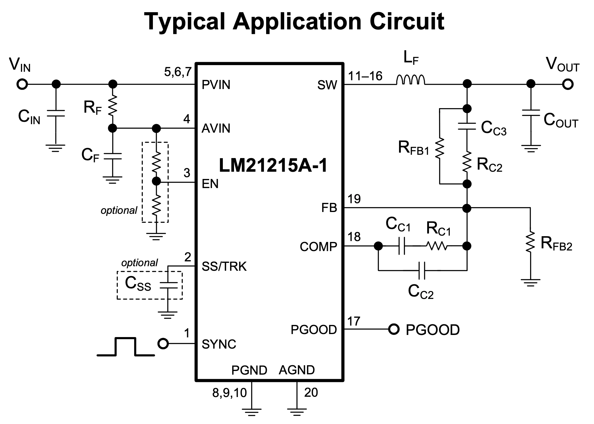
Ref. 1 shows the datasheet from TI (Texas Instruments). It is a 2.95-V to 5.5-V,15-A, Voltage-Mode Synchronous Buck Converter. The block diagram is as shown in Fig. 1.

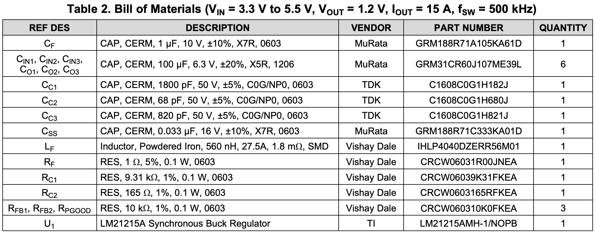
From LM21215A datasheet, we can get the following values in a typical application.

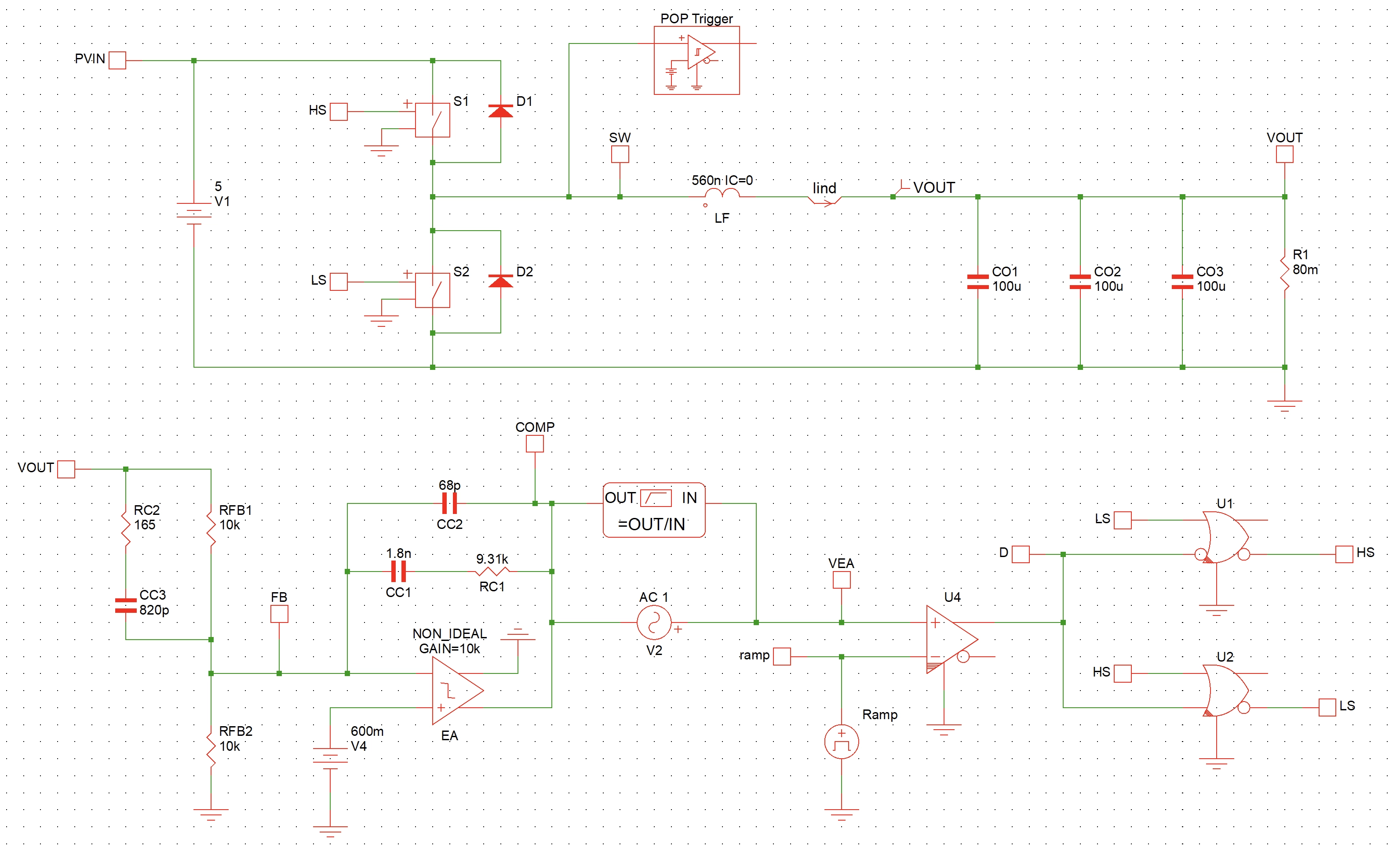
From there, we can create LM21215A model in Simplis as shown in Fig. 3.

The time domain waveforms are as shown in Fig. 4. The VOUT is regulated at 1.2V and the inductor current is the same as the load current, which is 15A.


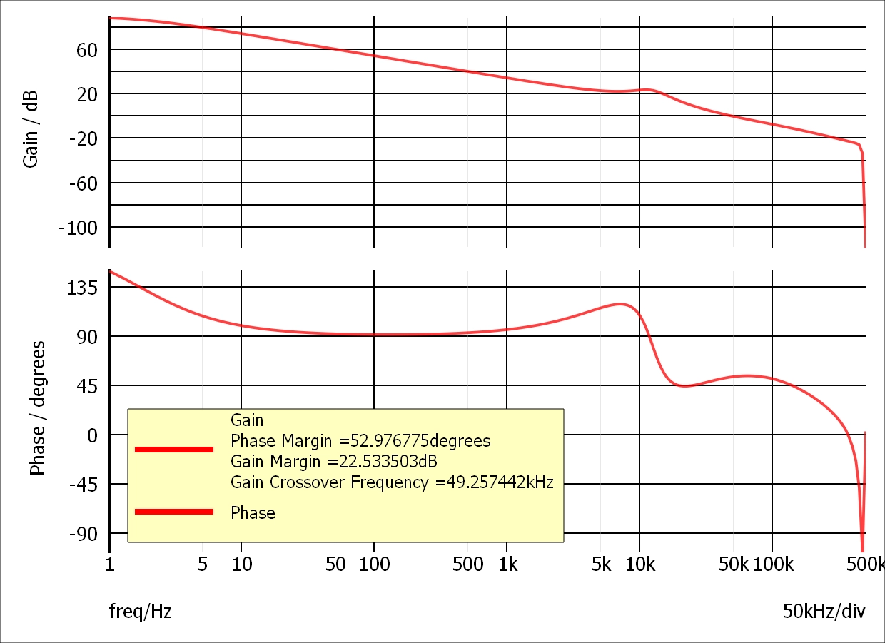
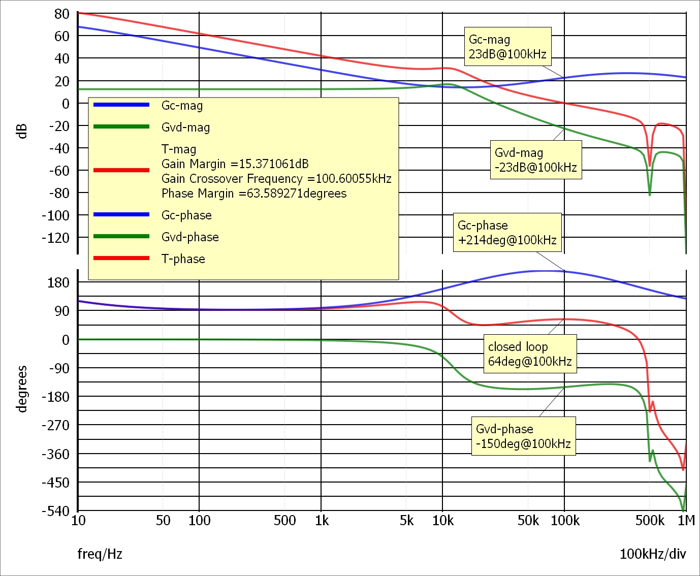
The closed loop Bode plot from AC simulation is as shown in Fig. 5.

Design procedure
Fig. 6 shows the pole and zero locations for the design procedure.

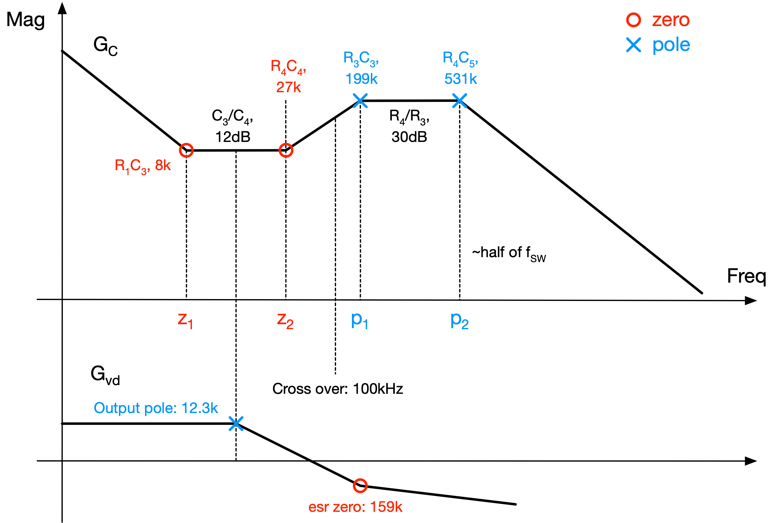
To summarize the pole and zero locations:
- The output complexed poles are placed between the two zeros formed by R1C3 and R4C4.
- The cross over frequency is placed between R4C4 and R3C3.
- The pole formed by R3C3 is placed near the esr zero so that they can cancell with each other.
- The pole formed by R4C5 is placed near half of the switching frequency.
The closed-loop voltage-mode Buck converter model is as shown in Fig. 7. Given the compensation network components value, every resistor and capacitor from the Type-III compensator should be able to be integrated into the silicon.

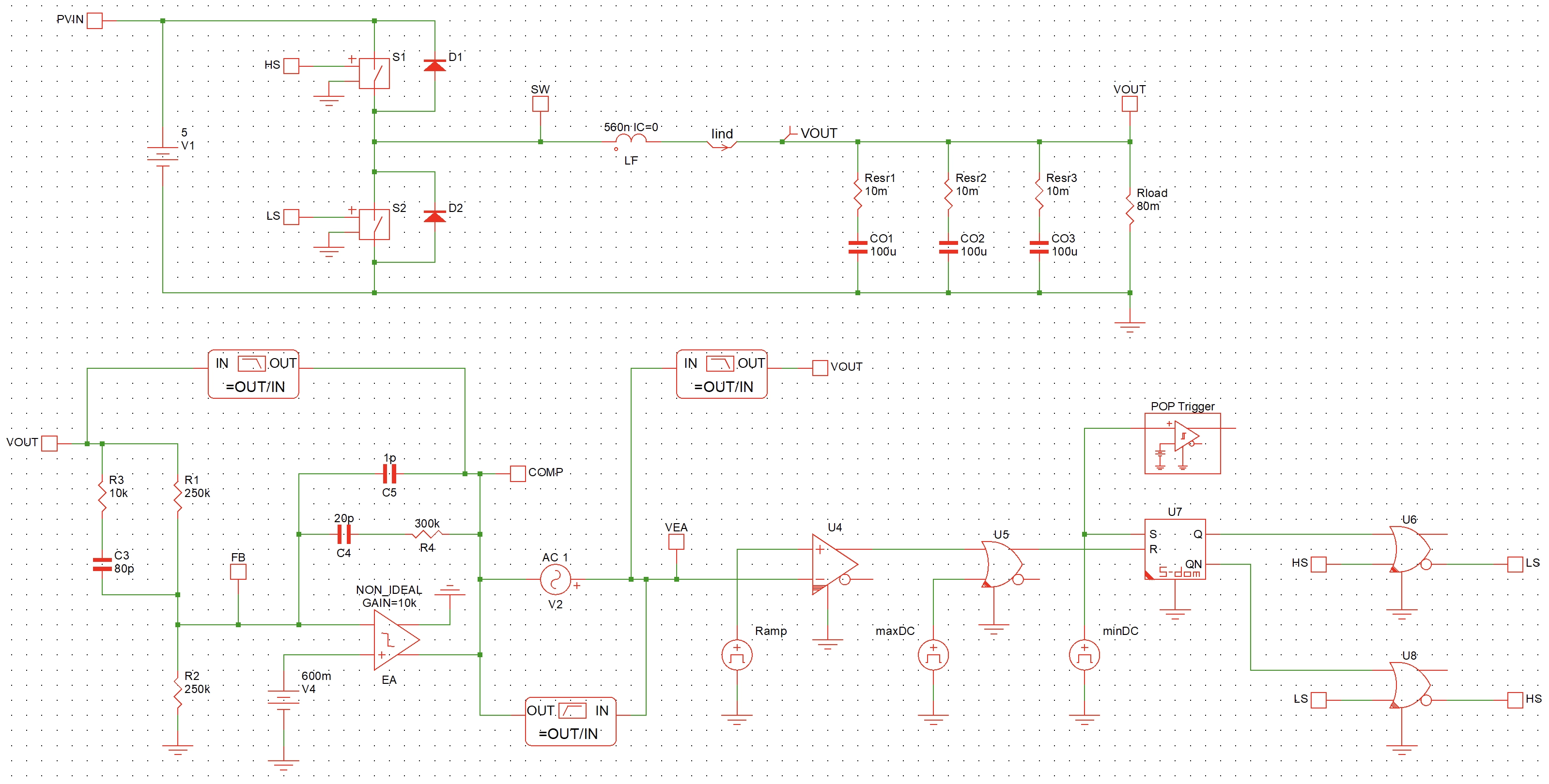
Fig. 8 shows the Bode plot of Gc (compensation network), Gvd (duty cycle to output) and closed-loop transfer function.

References and downloads
[2] Power stage transfer function cheatsheet - Voltage Mode
[3] Type-III compensator design tutorial
[4] LM21215A model in Simplis - pdf
[5] LM21215A model in Simplis - download
[6] Redesigning LM21215A compensation network in Simplis - pdf
[7] Redesigning LM21215A compensation network in Simplis - download