PCM (Peak current mode) controlled Boost converter design example


Ming Sun / December 23, 2022
10 min read • ––– views
Conditions
- Vin = 3.8V
- Vout = 20V
- R = 20Ω
- L = 1µH
- C = 10µF (derated)
- fsw = 3MHz
- Rsns = 0.3Ω
- Se tracks inductor current down-slope
Gvc transfer function for PCM (peak current mode) Boost converter
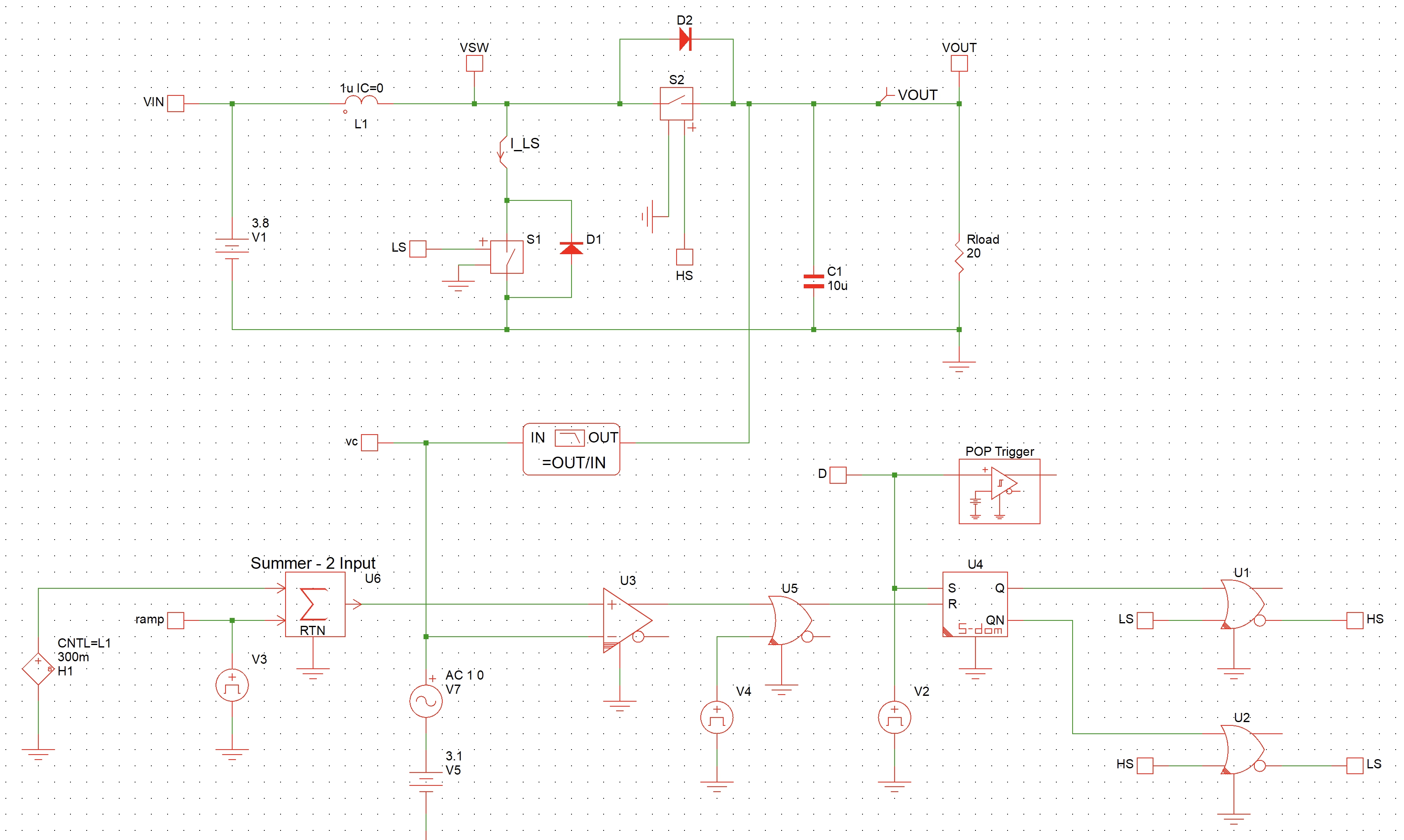
A PCM controlled Boost converter is as shown in Fig. 1[1].

We know that for a Boost converter, its right half plane zero can be expressed as:
Therefore, we can plug in the circuit conditions into Eq. 1. We have:
We know that right half plane zero can not be compensated in the frequency domain. This is because in order to compensate right half plane zero we need to have a right half plane pole, which does not exist in a stable circuit. Therefore, the closed loop cross over frequency of the PCM controlled Boost converter has to be less than the right half plane zero frequency. As a result, let us choose the cross over frequency to be 40kHz.
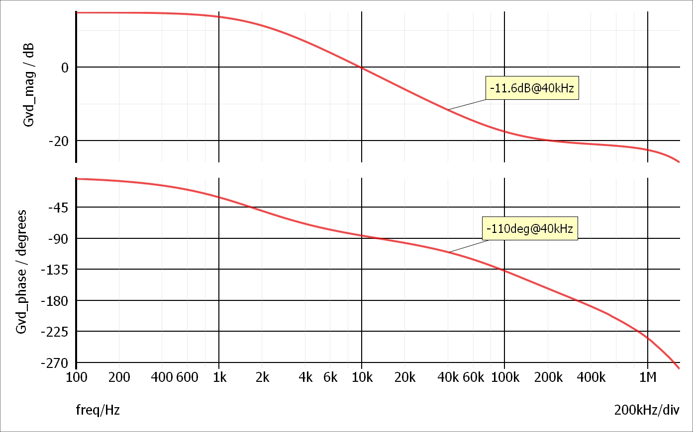
The Gvc transfer function simulated result is as shown in Fig. 2[1].

Next, we are going to design the Type-II compensator to make the PCM Boost converter stable.
Type-II compensator design
Fig. 3 shows a Type-II compensator, where an OTA is being used[3].


From Ref. [3], we can sketch the Type-II compensator transfer function as shown in Fig. 4.


p1 is the dominant pole, which will make sure we have a good DC voltage accuracy at Boost converter's output. Since we have a low frequency pole due to Gvc, z1 has to be placed inside the cross over frequency so that we can have sufficient phase margin. Let us place z1 to be 1/4 of the cross over frequency, which is 10kHz.
First, let us choose C1 to be 50pF and calculate the rest of the compensation network components value. If the calculated results do not quite make sense to integrate the components (resistors or capacitors) in the silicon, we can always come back to pick a new value for C1. As a result, the resistor R1 value can be calculated as:
We know the mid-band gain of the Type-II compensator is gm*R1. To make sure the cross over frequency is at 40kHz, from Fig. 2, we know that:
Where, α is the resistor feedback factor. Since output is 20V and typically bandgap voltage is 1.2V, the feedback factor can be calculated as:
As a result,
Let us place the p2 pole to be at switching frequency to suppress the ripple. Therefore, we have:
PCM closed loop model
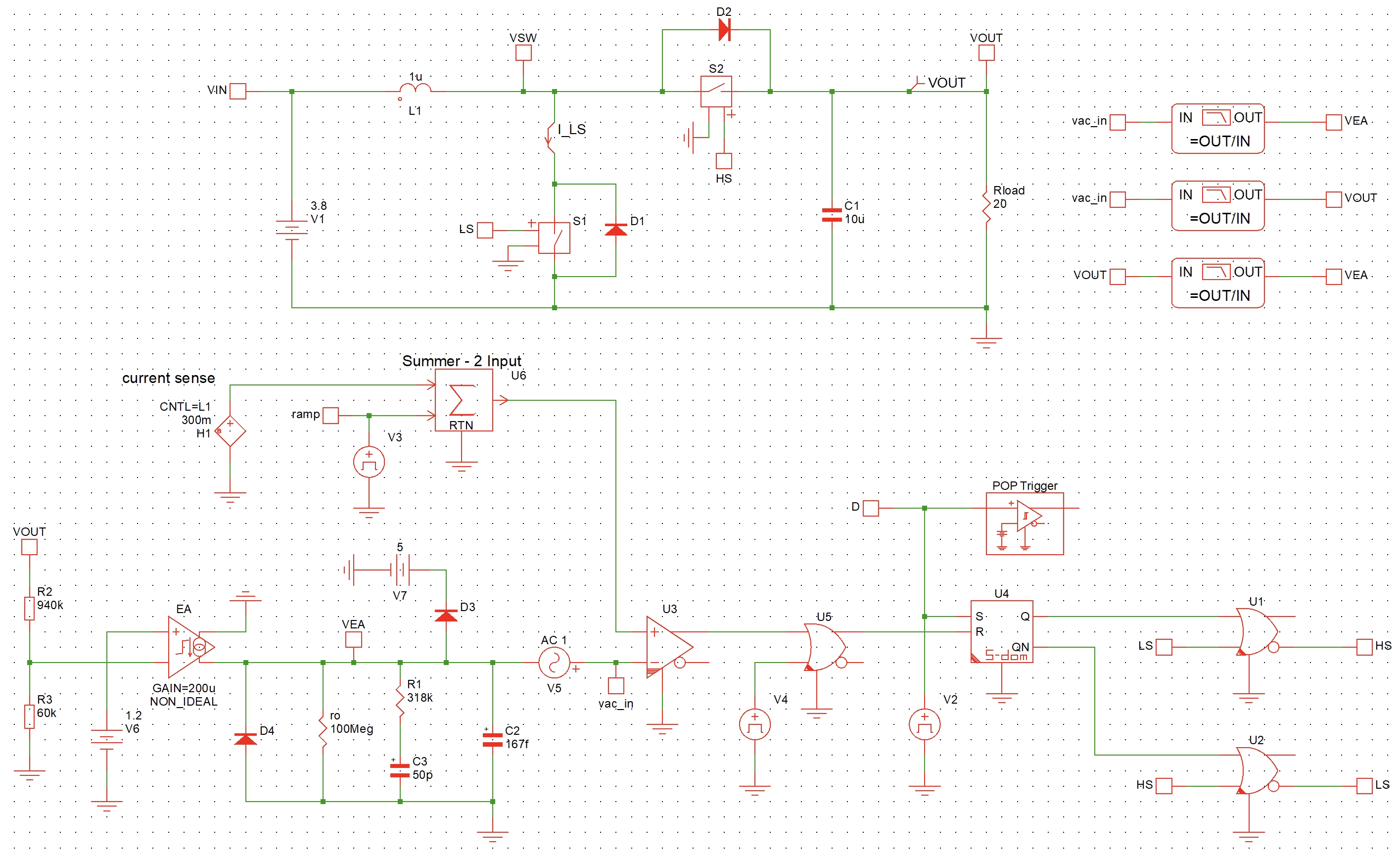
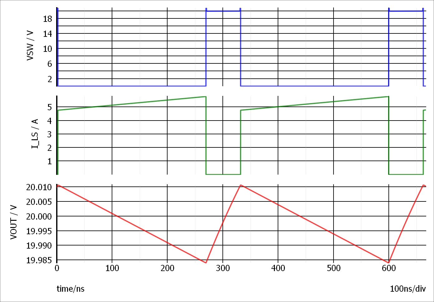
The PCM controlled Boost converter model in Simplis is as shown in Fig. 5.

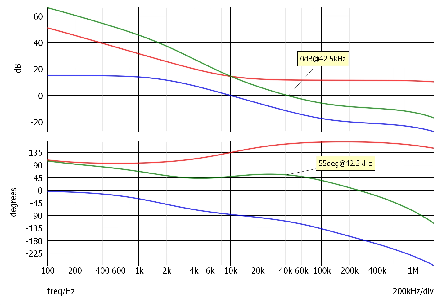
The closed-loop transfer function, compensation network transfer function and Gvc transfer function are as shown in Fig. 6.

The transient waveform is as shown in Fig. 7.

References and downloads
[1] Gvc simulation for peak current mode controlled Boost converter in Simplis
[2] Modeling of peak current mode controlled Boost converter
[3] Type-II compensator - OTA based