PCM (Peak current mode) controlled Buck converter design example


Ming Sun / December 24, 2022
13 min read • ––– views
Conditions
- Vin = 3.8V
- Vout = 1.8V
- R = 1.8Ω
- L = 1µH
- C = 10µF (derated)
- fsw = 3MHz
- Rsns = 0.3Ω
- Se tracks inductor current down-slope
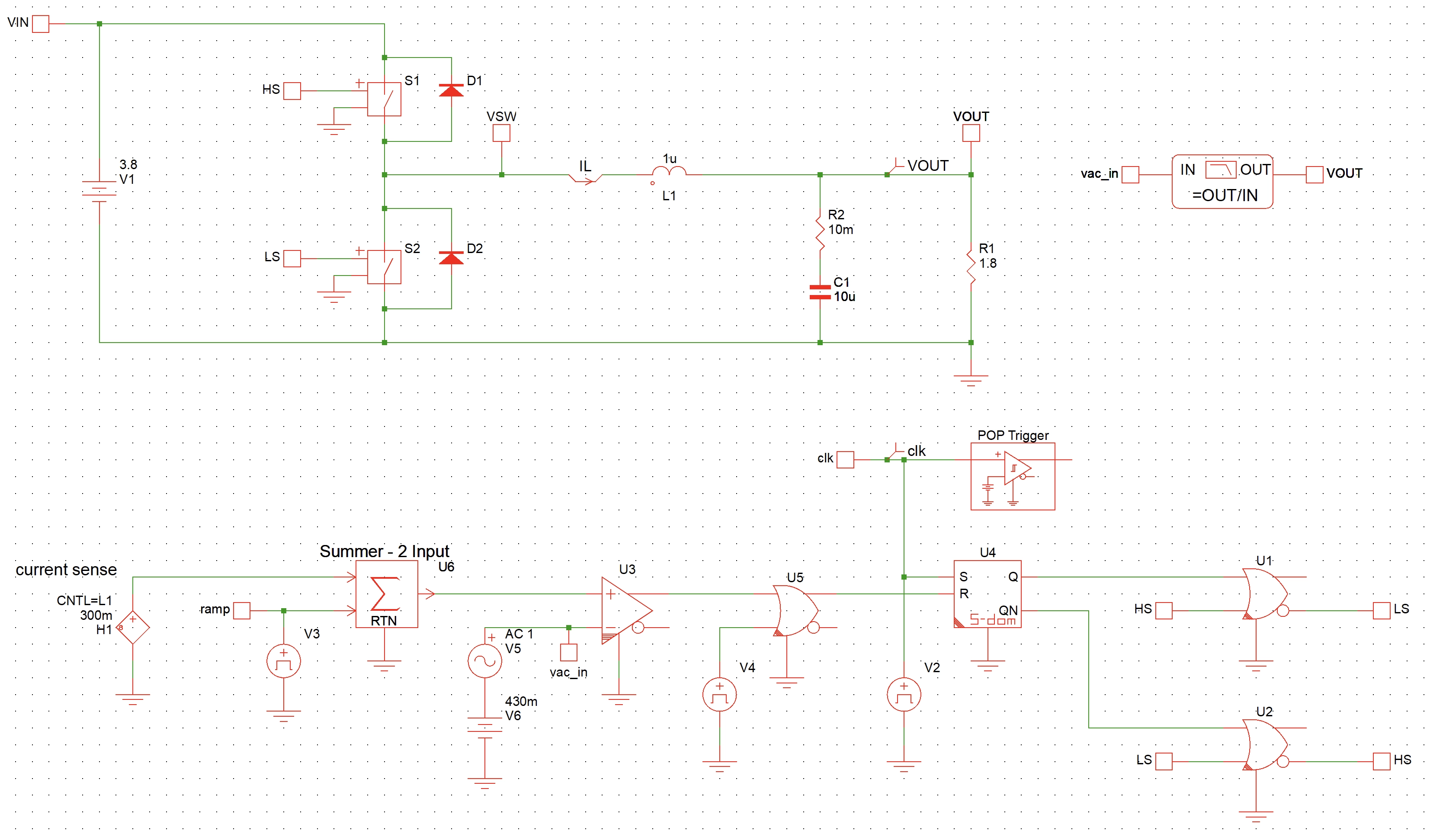
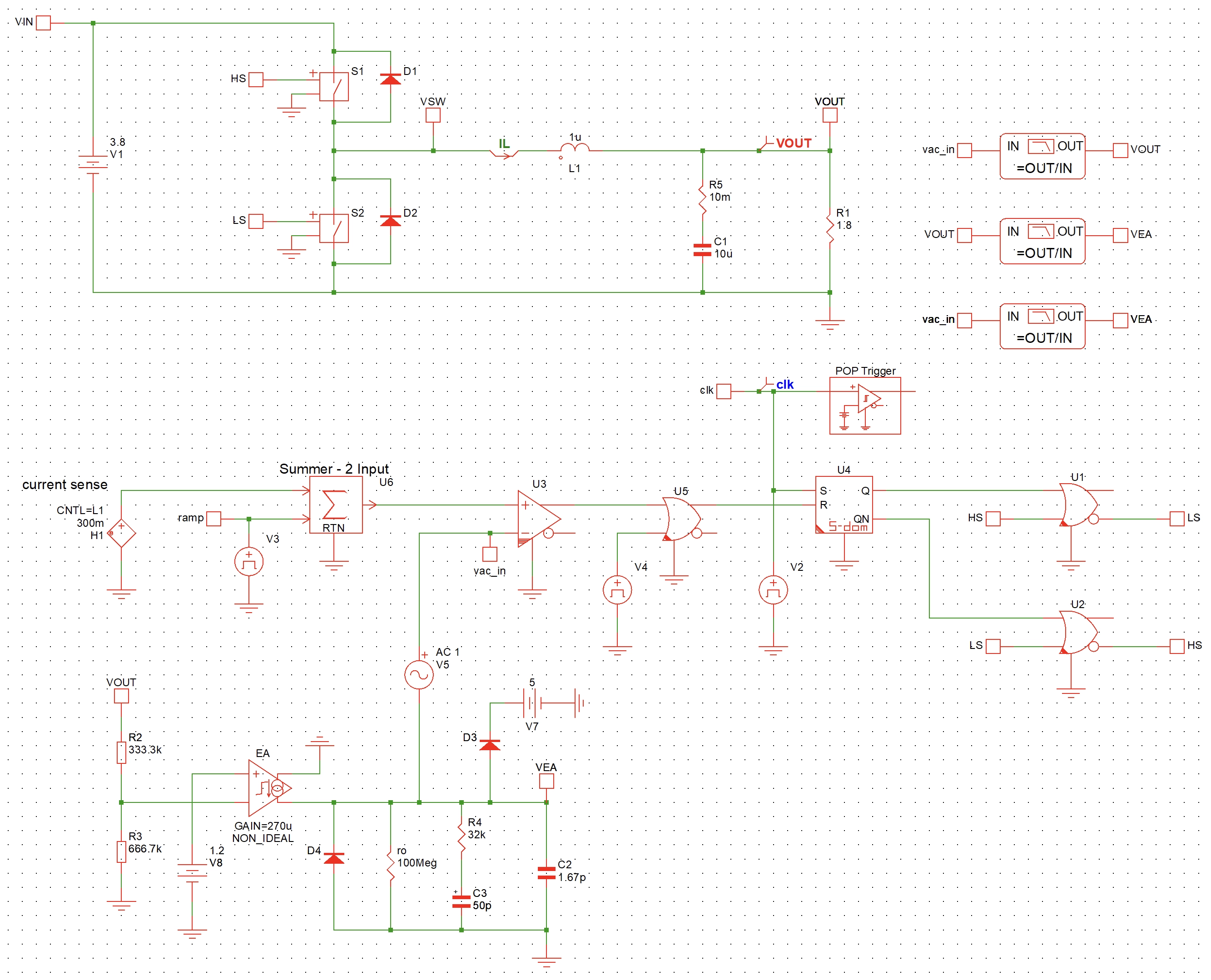
Gvc test bench in Simplis for PCM (peak current mode) Buck converter
In Ref. 1~2, we first derived the Gvc transfer function equation and then designed the Type-II compensator. In this tutorial, we are going to just use Simplis as a tool to design the closed loop transfer function. There is no necessary to derive the Gvc mathematically anymore.

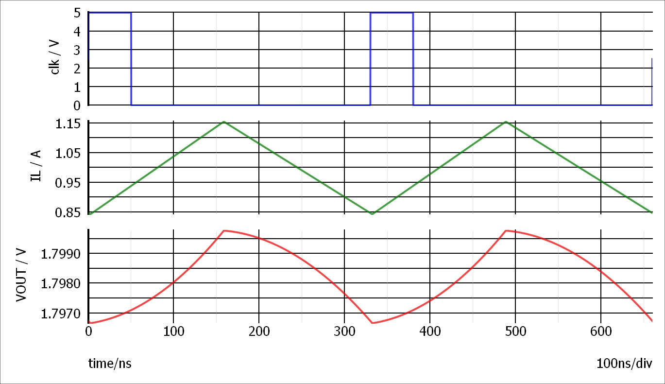
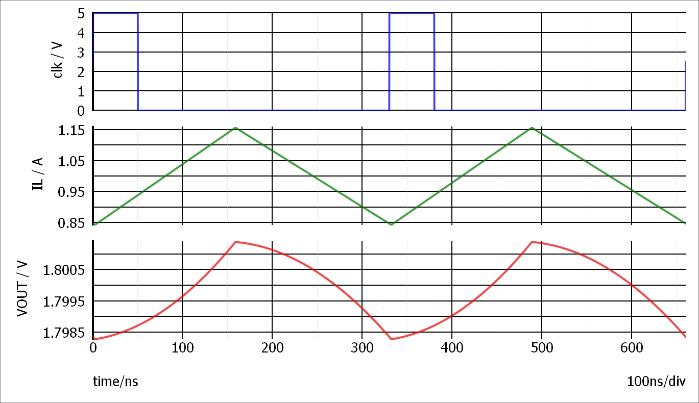
The transient waveforms from Simplis are as shown in Fig. 2.

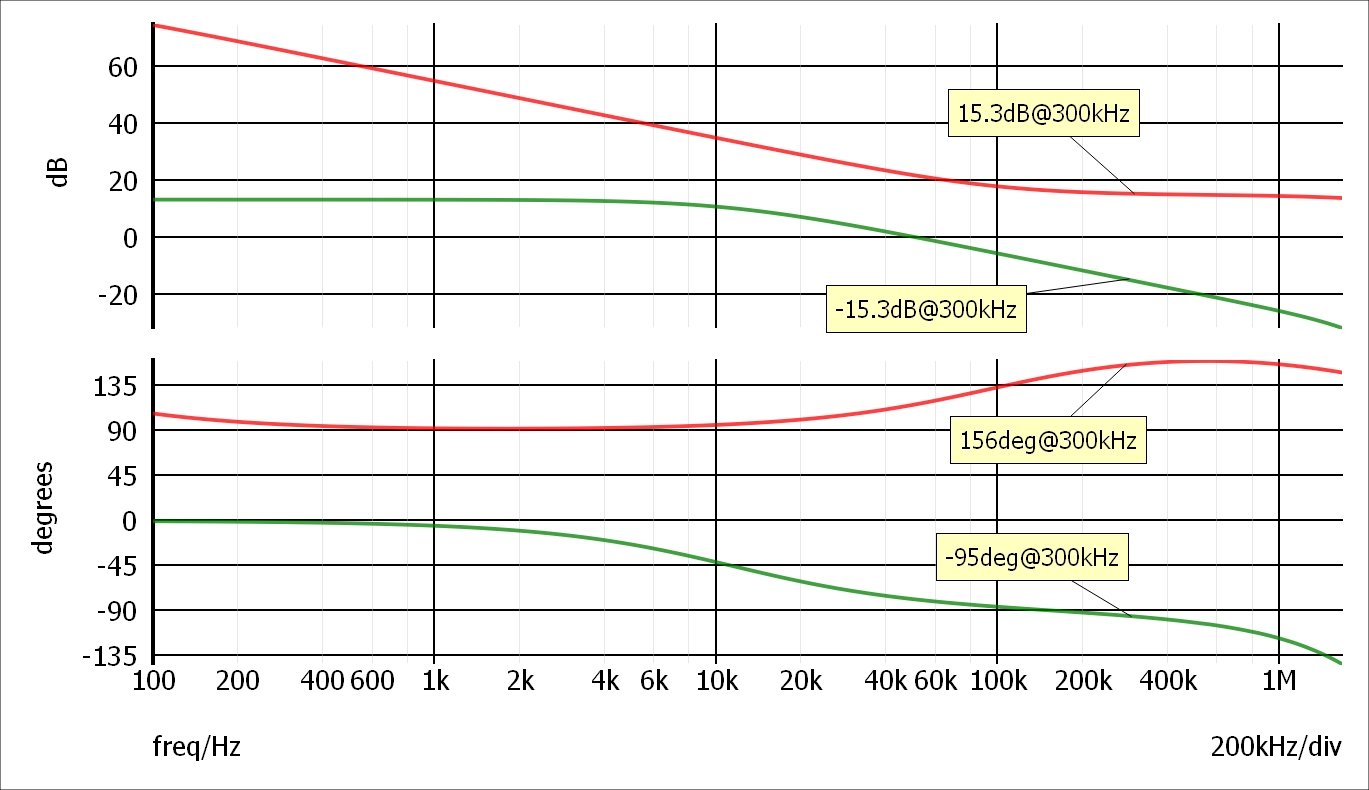
The Gvc simulation result from Simplis is as shown in Fig. 2.
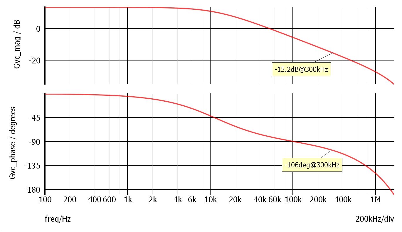
We have added two markers on the plot. For the Buck converter, we do not have the limitation of the right half plane zero. Therefore, the cross over frequency can be designed very high. Here our design target is to design the cross over frequency to be around 300kHz with reasonable amount of phase margin.
Design Type-II compensator
Fig. 4 shows a Type-II compensator, where an OTA is being used[3].


From Ref. [3], we can sketch the Type-II compensator transfer function as shown in Fig. 5.


p1 is the dominant pole, which will make sure we have a good DC voltage accuracy at Buck converter's output. Since we have a low frequency pole due to Gvc, z1 has to be placed inside the cross over frequency so that we can have sufficient phase margin. Let us place z1 to be 1/3 of the cross over frequency, which is 100kHz.
First, let us choose C1 to be 50pF and calculate the rest of the compensation network components value. If the calculated results do not quite make sense to integrate the components (resistors or capacitors) in the silicon, we can always come back to pick a new value for C1. As a result, the resistor R1 value can be calculated as:
We know the mid-band gain of the Type-II compensator is gm*R1. To make sure the cross over frequency is at 100kHz, from Fig. 3, we know that:
Where, α is the resistor feedback factor. Since output is 1.8V and typically bandgap voltage is 1.2V, the feedback factor can be calculated as:
As a result,
Let us place the p2 pole to be at switching frequency to suppress the ripple. Therefore, we have:
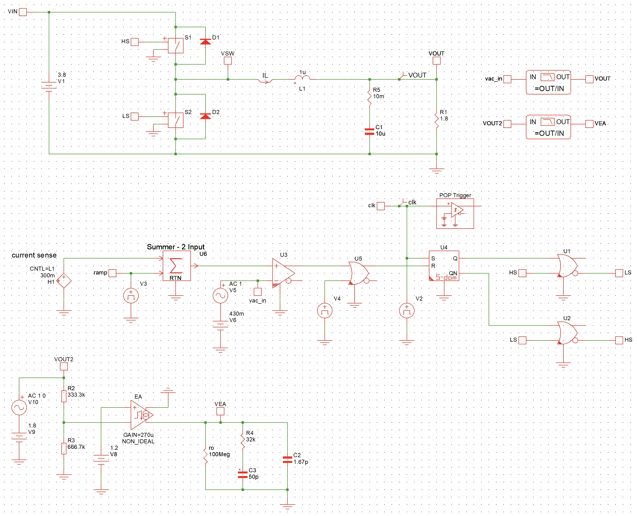
Add Type-II compensator into the Gvc test bench
Next, let us add the Type-II compensator into the Gvc test bench. However, we still keep the loop open. In this way, we can plot both the Gvc and Gc (compensator transfer function) into the same AC Bode plot. The schematic is as shown in Fig. 6.

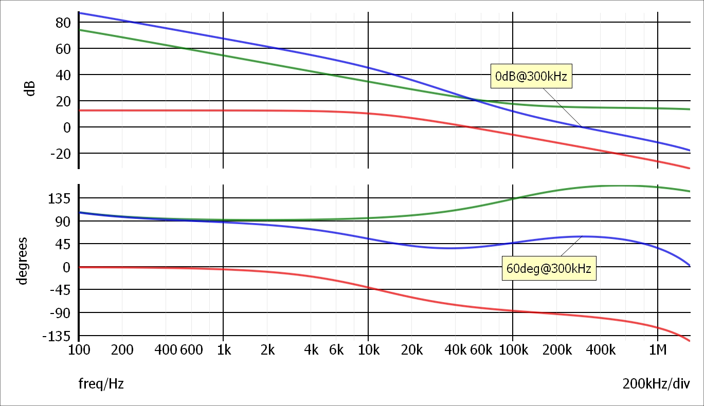
The Bode plot for Gvc and Gc is as shown in Fig. 7.

Closed-loop PCM Buck converter model
The closed-loop PCM Buck converter model in Simplis is as shown in Fig. 8.
The transient waveforms are as shown in Fig. 9.
The AC simulation results are as shown in Fig. 10.
References and downloads
[1] PCM (Peak current mode) controlled Boost converter design example
[2] Voltage-mode Buck converter design example
[3] Type-II compensator - OTA based
[4] Gvc test bench for PCM Buck in Simplis - pdf
[5] Gvc test bench for PCM Buck in Simplis - download